Gen 3.2
- General Microservers, Vexcel Microservers, Quick Reference, Data Acquisition, Middleware
- Components GPS, SBC
- Configuration Microserver, SBC, SD Card, Power
- Operation Communication Protocol (SBC <–> uc), SBC Operations, Agent
- Operation (background) Task Manager “milo”, config files, MACRO
- Microcontroller Microcontroller, Firmware, Skeleton firmware
- Evaluation 2008 Cairn relay failure evaluation, Lab evaluation, Eval-Firmware, BPMS, Source notes
- PCS Board PCS Board Design, Voltage Monitoring Circuit
Gen 3.1
- Gen 3.1 Kernel Upgrade and Field Notes (Spring 2007)
- Gen 3.1 Microserver, README, Schematics
- Gen 3.1 Task Manager “milo”, GPS, Firmware
Microcontroller-related
Other Microserver-Related
Introduction
The purpose of this page is to document the Vexcel microserver Power Conditioning Subsystem (PCS).
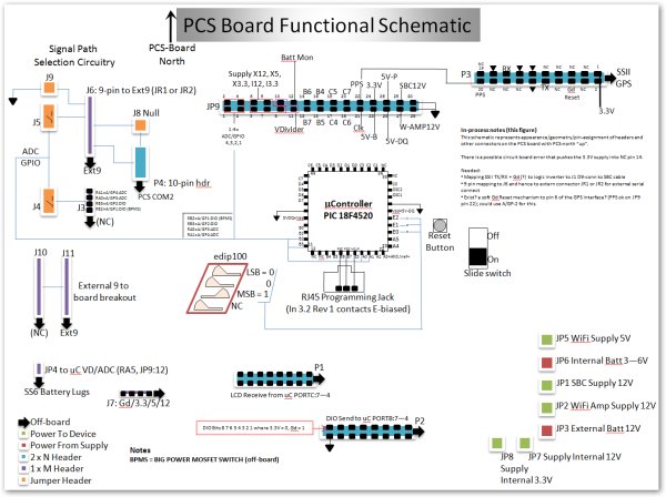
Reference figures
This diagram shows the PCS board “fragmented” to accommodate a spatial representation of different functions. Any orange in the graphic indicates that the part or functionality is located on the PCS board.
This diagram is an approximation of the physical layout of the PCS board. It is intended as a working map (like the London subway map) where spatial relationships are approximate. Connectors and headers are labeled on the board and can be referenced to their labels here.
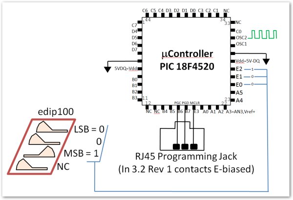
This diagram is a detail from the previous diagram. It gives the PCS microcontroller pinout, where the device is a Microchip PIC 18LF4520.
PCS 0 Best practice and precautions
Indicate power on/off rules, broken aspects of the early Gen 3.2 board…
PCS 1 Power Connectors
Must include J7 here.
PCS 2 Power Monitoring
Include JP4 and define SS6.
PCS 3 GPS Interface
Includes P3 and serial connection to COM1 on SBC
PCS 4 SBC Interface
4 bits used out of 8 in both directions, LCD = PORTC, DIO = PORTB, programming note on setting values
PCS 5 Microcontroller Programming
This has to include the RJ45 and edip switch. Note in diagram how edip 100 maps to uC pins
PCS 6 Signal Path Selection
Explicit ADC/GPIO stuff.
PCS 7 JP9 Test Header
Include note on spare voltage divider
For more detail: Gen 3.2 PCS Board Design