Summary of ELECTROMAGNETIC NEAR-FIELD PCB PROBES ARE OPEN SOURCE
Summary: Near-field scanning identifies PCB electromagnetic interference (EMI) sources to assess electromagnetic compatibility (EMC). In the near-field region, electric and magnetic fields can act independently; E-field and H-field probes measure localized electric and magnetic strengths respectively. E-field probes use short dipole antennas, detector diodes, non-perturbing transmission lines, and readouts (often three orthogonal dipoles or optical fiber links). H-field probes use PCB magnetic loops and transmission lines (commonly microstrip) to convey induced HF waveforms to receivers.
Parts used in the Electromagnetic Near-Field PCB Probes project:
- Short dipole antenna
- Detector diode
- Non-perturbing transmission line
- Readout device
- Optical fiber and modulated light source (optional data link)
- Printed circuit magnetic loop
- Transmission line (mostly microstrip line)
- Three orthogonal dipoles (for isotropic E-field response)
In modern compact electronic circuits, there are several components on a confined PCB area, and so, the electromagnetic effects induced from one component may affect the surrounding components. This disturbance is known as Electromagnetic Interference (EMI).
The source of the radiation must be identified in PCBs to predict the EMC of electronic circuits. Electromagnetic compatibility (EMC) is the ability of electrical equipment and systems to function acceptably in their electromagnetic environment, by limiting the unintentional generation, propagation, and reception of electromagnetic energy which may cause unwanted effects such as EMI. Near-field scanning is the general method for identifying radiation sources in PCBs.
Electromagnetic Near-Field Scanning
Near-field scanning is used for estimating localized electromagnetic emissions. The far-field is a region in which the field acts as normal electromagnetic radiation. But in the near-field region, electric and magnetic fields can exist independently. Additionally, in the near-field region, one type of field can dominate the other. E-field and H-field probes are used for electromagnetic near-field scanning. E-field probe measures point-to-point the electric field strengths locally. On the other hand, the H-field probe measures the magnetic field strengths locally.
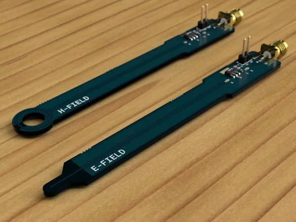
E-Field And H-Field Probes: An Overview
The E-field probe consists of a short dipole antenna, a detector diode, a non-perturbing transmission line, and a readout device. Three orthogonal dipoles are generally used in an E -field probe to provide a response that is nearly isotropic for all polarizations of the incident field. Optical fibers, together with a suitably modulated light source, may be used to form a wide-band non-perturbing data link from the dipole and detector to a remote readout [1].
The H-field probe consists of a printed circuit magnetic loop and a transmission line. The magnetic flux from the loop will induce a high-frequency waveform that travels through a transmission line to the receiver. The transmission line is mostly a microstrip line.
Read more: ELECTROMAGNETIC NEAR-FIELD PCB PROBES ARE OPEN SOURCE
- What is electromagnetic interference in PCBs?
Electromagnetic interference is the disturbance where electromagnetic effects from one component affect surrounding components on a confined PCB area. - How is the source of radiation identified in PCBs?
The source is identified using near-field scanning to estimate localized electromagnetic emissions. - What is electromagnetic compatibility (EMC)?
EMC is the ability of equipment to function acceptably in its electromagnetic environment by limiting unintentional generation, propagation, and reception of electromagnetic energy. - How do E-field probes work?
E-field probes use short dipole antennas, a detector diode, a non-perturbing transmission line, and a readout device to measure local electric field strengths. - Why are three orthogonal dipoles used in an E-field probe?
Three orthogonal dipoles provide a response nearly isotropic for all polarizations of the incident field. - Can optical fibers be used with E-field probes?
Yes, optical fibers with a modulated light source can form a wide-band non-perturbing data link from the dipole and detector to a remote readout. - How do H-field probes measure magnetic fields?
H-field probes use a printed circuit magnetic loop that induces a high-frequency waveform conveyed through a transmission line to the receiver. - What transmission line is commonly used with H-field probes?
The transmission line is mostly a microstrip line.