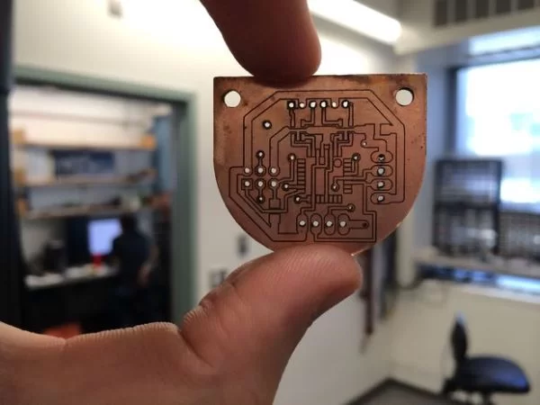
With a little practice, you can make excellent double-sided PCBs by combining a laser cutter with chemical etching. The basic idea is: the laser cutter blasts away spray painted etch resist, then chemicals eat away the exposed copper. Once the copper is gone, the underlying board can be cut again with the laser to make through-holes. No drilling required! After some setup and practice, you should get reliable boards with 8-mil trace/space and hundreds of holes in about 2 hours. You can even cut internal routing and odd board-shapes!
You’d never want to make a bunch of boards this way, but if you want a same-day prototype of a new design it’s perfect. I love this process because I don’t have to wait 2 weeks for boards to come back from fab, so I can design aggressively and try new ideas. If you’re in a research lab or shop you’ll have no trouble finding the materials, but you should also be able to find everything you need at a hardware store and pharmacy.
This Instructable will go step-by-step through the process of making a double-sided board, with special attention paid to using software to generate a good laser path, and some neat tricks to help get good alignment between the top and bottom sides of the board. Drop me a note if you’ve got feedback or new ideas!
The steps are:
(1) Coat PCB stock with spray paint
(2) Laser cut a spring-form alignment jig
(3) Optimize your board layout for fabrication
(4) Generate vector art for the cutter
(5) Etch away black spray paint with the laser on both sides
(6) Chemically etch away exposed copper
(7) Laser cut through-holes in the exposed board
(8) Tricks and tips for soldering DIY boards
Stuff you’ll need:
Access to a laser cutter
FR1 PCB blanks (try www.inventables.com)
Spray paint (McMaster #7719T9)
6″x6″ of acrylic between 1/8″ and 1/4″ thick (3 mm – 6 mm) for making a jig
Drill press or rotary tool with small bit (optional, but helpful for alignment)
Gloves, goggles
Non-metallic dish, measuring device, and tools
Hydrogen peroxide (3%)
Hydrochloric acid (30-37%, also called muratic acid)
Paper towels
You’ll also need some access to software:
A PCB design, exported to a format your graphics program can read (I use Eagle exporting to EPS)
A vector graphics program to edit the art in. I used Adobe Illustrator.
A brief note on safety and the environment:
If you have access to a laser cutter you should be familiar with the dangers involved with that. But these instructions also guide you through copper chloride etching, which you may not be familiar with. The chemicals used are dangerous. Hydrochloric acid can burn your skin, blind you, and generates poisonous fumes. The hydrogen peroxide is reactive with lots of stuff, and the heavy metals (copper) are poisonous. Always work outside (or in a chemical fume hood), in gloves and goggles. And make sure you have adult supervision if you’re under the age of, say, 40.
Finally don’t put your etch waste down the drain – it will poison both people and the environment. Store it safely in a labelled container, and dispose of it properly by contacting a hazardous waste disposal agency in your area.
For more detail: Double-sided PCBs with a laser cutter