Some time ago I sourced a number of very cheap SD card sockets from China for a hobby project I was working on. Sadly, when it came to PCB design, I couldn’t find the footprints for this particular socket anywhere – the part being a proprietary invention of the factory rather than a cheap knockoff of a reputable brand like Amphenol or Molex for which drawings are readily available off of snapeda.com.
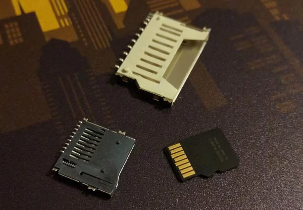
Turns out, this is a problem with many, many parts – there are no CAD drawings to be found anywhere, and the only way to really fit the part onto a board is to measure the part and draw everything yourself – a tedious manual process, but with a few tools, any part can be precisely drawn and transferred onto the board.
Step one – Scan the part using a flatbed scanner
In the absence of other tools, one can use any flatbed scanner to reproduce the measurements required to draw a part. At 300dpi, a scan will yield a sufficient measurement on most, if not all parts. One key thing to remember is to ensure that each part is aligned with the edge of the scanner – I’ve managed to accomplish this, using a public transport card I’ve found in my drawer. Simply place the card (or any other rectangular item) next to the edge, and make sure it touches it and is aligned with it, then – align your parts with the edges of the card. The alternative is to use the edges of the scanner to align the parts, but I’ve found that to be unreliable.
Read more: Creating footprints in KiCad using a scanner