Summary of Building a PIC18C and System-on-a-Chip in an FPGA
The PIC18C project involves designing a synthesizable VHDL model of the Microchip PIC18C microcontroller, verifying it with assembly and C programs, and implementing it on an FPGA. The core is fully compatible with the PIC18 series, enabling high-level language development.
Parts used in the PIC18C FPGA Project:
- Data Processing Unit (DPU)
- Arithmetic-Logic Unit (ALU)
- Multiplier
- Rotater
- Bit-Operation Processor (BOP)
- Instruction Decoder
- Fetcher
- Instruction Register
- Program Counter
- Hardware Return Stack
- Block RAM
- Constant Data Fetcher
- Register File
- Reset
- Watchdog Timer
- ROM
- Spartan-II Development Kit
- Xilinx Spartan-II XC2S100 FPGA
- Standard text-based LCD module
- MPLAB development system
Description
The goal of the PIC18C project is to design, develop a synthesizible VHDL model, verify it using test programs, and implement a core of the Microchip PIC18C microcontroller. The microcontroller core is fully compatibile with the PIC18 series allowing program development using high-level programming languages such as C.
The project phases are described below.
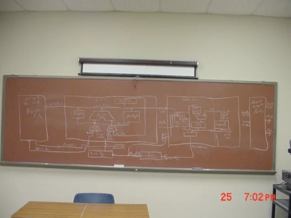
1. Design
The design phase involves the detailed study of the architecture and instruction set. The key elements of the architecture are defined: instruction fetcher, decoder, register file, etc. The instruction set is examined and grouped to facilitate decoding.
2. VHDL Model Development
The key architectural components derived from the design phase are used to form the VHDL model hierarchy. The hierarchy is shown below.
PIC
Data Processing Unit (DPU)
Arithmetic-Logic Unit (ALU)
Multiplier
Rotater
Bit-Operation Processor (BOP)
Instruction Decoder
Fetcher
Instruction Register
Program Counter
Hardware Return Stack
Block RAM
Constant Data Fetcher
Register File
Block RAM
Reset
Watchdog Timer
ROM
Block RAM
3. Verification
The initial PIC operation verification is done by writing a single assembly language test file for each instruction. The program was assembled using Microchip’s MPLAB development system. A simple C program is used to convert the output of the Assembler (HEX format) into a format suitable for cut-and-paste into the ROM array.
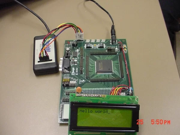
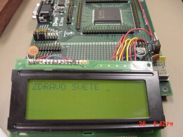
4. Implementation & Demonstation
The PIC is sucessfully synthesized and implemented using Spartan-II Development Kit with Xilinx Spartan-II XC2S100 FPGA. The PIC operation is demonstrated by displaying a “Hello world” type string onto a standard text-based LCD module. This milestone is reached on April 20th.
Photo Album
Source: Building a PIC18C and System-on-a-Chip in an FPGA
-
What is the primary goal of the PIC18C project?
The goal is to design, develop a synthesizable VHDL model, verify it using test programs, and implement a core of the Microchip PIC18C microcontroller. -
How is the microcontroller core verified?
Verification is done by writing a single assembly language test file for each instruction and using a simple C program to convert assembler output into a format for the ROM array. -
Which hardware platform was used for implementation?
The PIC was successfully synthesized and implemented using the Spartan-II Development Kit with Xilinx Spartan-II XC2S100 FPGA. -
Can the core be programmed using high-level languages?
Yes, the microcontroller core is fully compatible with the PIC18 series allowing program development using high-level programming languages such as C. -
What tool was used to assemble the test programs?
The program was assembled using Microchip's MPLAB development system. -
What demonstration was performed after implementation?
The PIC operation was demonstrated by displaying a Hello world type string onto a standard text-based LCD module. -
What are the key architectural elements defined in the design phase?
The key elements include the instruction fetcher, decoder, register file, and the instruction set which is examined and grouped to facilitate decoding. -
How was the assembler output prepared for the ROM array?
A simple C program was used to convert the output of the Assembler in HEX format into a format suitable for cut-and-paste into the ROM array.