Summary of AI COMPUTE ACCELERATION STARTUP BUILDS THE LARGEST CHIP EVER FOR DEEP LEARNING APPLICATIONS
Cerebras Systems unveiled the Wafer-Scale Engine (WSE), the world's largest AI chip, measuring 46,225 mm² with over 1.2 trillion transistors. This single-wafer chip integrates 400,000 AI-optimized cores connected via a high-speed mesh network and features 18GB of on-chip SRAM. Designed specifically for deep learning, the WSE reduces complex data processing time from months to minutes while offering superior performance and power efficiency compared to existing GPUs.
Parts used in the Wafer-Scale Engine:
- Wafer-Scale Engine chip
- Sparse Linear Algebra cores
- Mesh communication network
- On-chip SRAM memory
- Silicon wafer substrate
To meet the ever-increasing computational demands of AI, California based AI startup, Cerebras Systems, just recently unveiled its very first announced element claimed to be the most massive AI chip ever made. With an astounding measurement of 46,225 mm2 (up to 56.7 times more than the largest graphics processing unit) and more than 1.2 trillion transistors, the Wafer-Scale Engine from Cerebras Systems is the largest semiconductor ever built for deep learning applications.
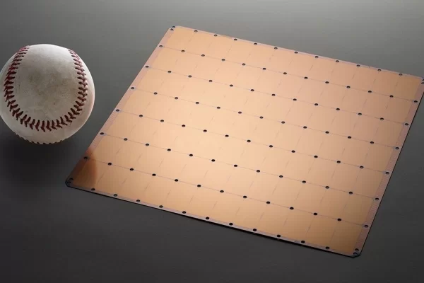
The Wafer-Scale Engine contains about 400,000 high performance, AI optimized Sparse Linear Algebra cores. This local memory fed cores are linked together by a fine-grained, high bandwidth, all-hardware, low latency mesh communication network at an interconnect speed of 100,000 Pb/s. Unlike other processors and GPUs that are produced on silicon wafers, Cerebras’ WSE is a single chip interconnected in a single wafer designed to handle all its transistors. The WSE also houses on-chip of 18Gb superfast and distributed SRAM memory among the cores in a single-level hierarchy. By way of comparison, the WSE has 3000 more on-chip memory and more than 10,000 times the memory bandwidth.
Designed for accelerating AI work, the company claims that its Wafer-Scale Engine can scale down the time it takes to process complex data from months to minutes.
“Every architectural decision was made to optimize performance for AI work. Designed from the ground up for AI work, the Cerebras WSE contains fundamental innovations that advance the state-of-the-art by solving decades-old technical challenges that limited chip size such as cross – reticle connectivity, yield, power delivery and packaging. The result is that the Cerebras WSE delivers, depending on workload, hundreds or thousands of times the performance of existing solutions at a tiny fraction of the power draw and space,”
Read more: AI COMPUTE ACCELERATION STARTUP BUILDS THE LARGEST CHIP EVER FOR DEEP LEARNING APPLICATIONS
- What is the size of the Cerebras Wafer-Scale Engine?
The chip measures 46,225 mm². - How many transistors does the WSE contain?
It contains more than 1.2 trillion transistors. - Does the WSE use multiple chips or a single wafer?
It is designed as a single chip interconnected within a single wafer. - What is the interconnect speed of the mesh network?
The interconnect speed is 100,000 Pb/s. - How much on-chip memory does the engine have?
It houses 18GB of superfast distributed SRAM memory. - Can the WSE reduce AI processing time significantly?
Yes, it claims to scale down processing time from months to minutes. - How does the WSE compare to GPUs in terms of memory bandwidth?
It has more than 10,000 times the memory bandwidth of comparable solutions. - What technical challenges did Cerebras solve to build this chip?
They solved challenges regarding cross-reticle connectivity, yield, power delivery, and packaging.