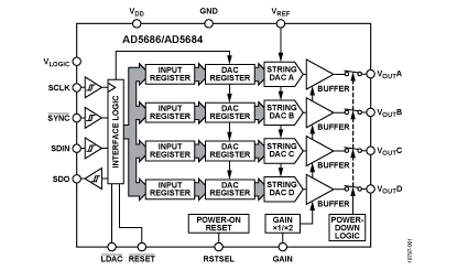
The AD5686, a member of the nanoDAC+™ family is a low power, quad, 16-bit buffered voltage output DAC. The device includes a gain select pin giving a full-scale output of 0V to VREF (gain = 1) or 0V to 2VREF (gain = 2). The device operates from a single 2.7 V to 5.5 V supply, is guaranteed monotonic by design, and exhibits less than 0.1% FSR gain error and 1.5 mV offset error performance. The device is available in a 3 mm × 3 mm LFCSP and a TSSOP package.
The AD5686 also incorporates a power-on reset circuit and a RSTSEL pin that ensures that the DAC outputs power up to zero scale or midscale and remain at that level until a valid write takes place. Each part contains a per-channel power-down feature that reduces the current consumption of the device to 4 µA at 3 V while in power-down mode.
The AD5686 employs a versatile SPI interface that operates at clock rates up to 50 MHz, and all devices contain a VLOGIC pin intended for 1.8 V/3 V/5 V logic.
FEATURES and BENEFITS
- High relative accuracy (INL): ±2 LSB maximum @ 16 bits
- Tiny package: 3 mm × 3 mm, 16-lead LFCSP
- Total unadjusted error (TUE): ±0.1% of FSR maximum
- Offset error: ±1.5 mV maximum
- Gain error: ±0.1% of FSR maximum
- High drive capability: 20 mA, 0.5 V from supply rails
- User selectable gain of 1 or 2 (GAIN pin)
- Reset to zero scale or midscale (RSTSEL pin)
- 1.8 V logic compatibility
- 50 MHz SPI with readback or daisy chain
- Low glitch: 0.5 nV-sec
- Robust 4 kV HBM and 1.5 kV FICDM ESD rating
- Low power: 1.8 mW at 3 V
- 2.7 V to 5.5 V power supply
- −40°C to +105°C temperature range
Analog Devices has a range of quad 16- and 12-bit 3V/5V digital-to-analogue converters (DACs) in its smallest 3mm x 3mm package.
The AD5686/96 nanoDAC+ quad DACs offer the supplier’s best DC performance specitiofcation. INL is ±2LSB max, offset error is ±1.5mV max and gain error is ±0.1% max in the LFCSP package with SPI or I²C interface options.
Applications are likely to include PLC (programmable logic controller) I/O cards, digital oscilloscopes, signal generators and optical modules that require low power, rail-to-rail.
The supplier’s AD5316R and AD5317R quad 10-bit nanoDACs offer similar DC performance to the AD5686/96, robustness up to 4kV ESD and low drift on-chip 2.5V voltage reference in a 3mm x 3mm footprint.
View the AD5686 D/A converter product page, order samples and eval boards and download the data sheet: http://www.analog.com/ad5686
For more read: ADI squeezes quad DAC into small 3mm x 3mm package

