Summary of PIC12 ADC Converter using PIC12C671 with Proteus Simulation
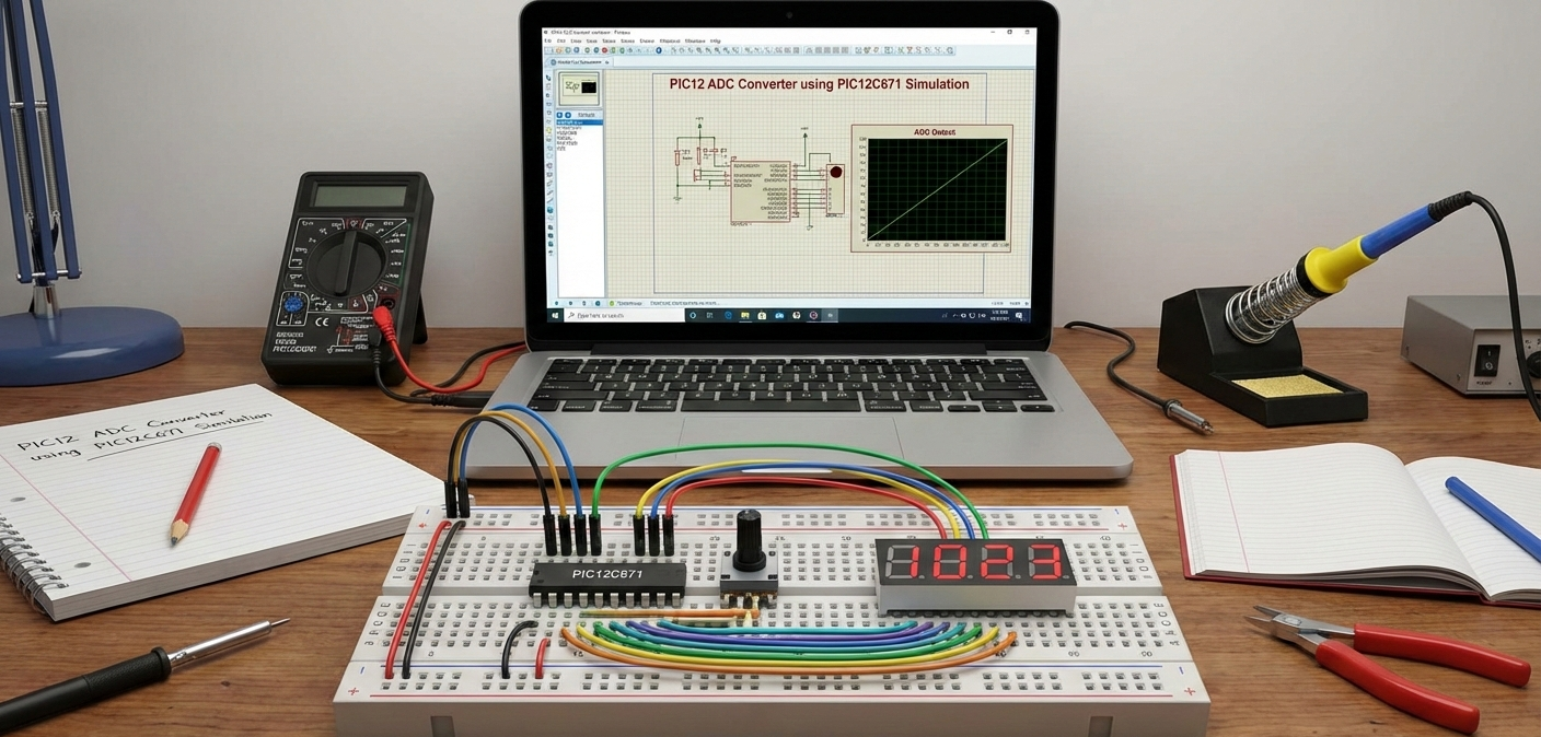
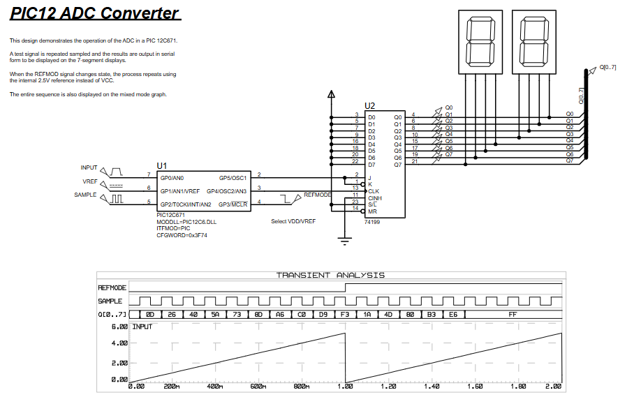
The PIC12 ADC Converter project demonstrates using the PIC12C671 internal ADC to sample an analog input, convert it to an 8-bit value, and serially shift that result out to external latch and dual 7-segment displays. It supports runtime selection of VDD or external VREF, uses interrupt-driven ADC completion, and is fully simulated in Proteus for visualization and learning.
Parts used in the PIC12 ADC Converter:
- PIC12C671 microcontroller
- External voltage reference source (VREF)
- Serial latch IC
- Dual 7-segment displays
- Clock and sample control signal sources
- Proteus VSM environment for simulation
- Why use PIC12C671 for ADC projects?
Because it provides a simple ADC module with minimal pin usage, making it ideal for learning. - Can this work with other PIC12 devices?
Yes, with minor ADC register and pin configuration changes. - Why is sleep mode used frequently?
It reduces power usage and lets the MCU wait efficiently for interrupts. - How is serial output implemented without UART?
GPIO pins manually shift data bit-by-bit using generated clock pulses. - Can I display ADC data differently?
Yes, LCDs or LEDs can be used instead of 7-segment displays. - Why does reference voltage matter?
It defines the ADC conversion range and affects conversion results. - Is this suitable for real hardware testing?
Yes, the logic directly maps to real PIC12C671 hardware.