Frustration!
Have you ever experienced frustration when you didn’t have a PIC programmer handy? Your programmer breaks or you loaned it out to your buddy and you sit just twiddling your thumbs. It left you feeling powerless because you couldn’t test that great idea, didn’t it? If so, you share experiences similar to mine. It is annoying at the very least and does not help creativity. Or maybe it does. It was that same frustration that finally led to my motivation for writing this article. Namely, not to ever feel helpless or powerless again (concerning PIC programming anyways).
The feeling of helplessness is not one I savor. But it really hurts that it’s through my own fault (basic laziness over the years) I was missing even the basic knowledge of how the programmer worked.
I realized I was so ignorant of the processes involved in programming the PIC that it felt like black magic. I resolved once and for all to remedy my ignorance. I was going to learn all I needed to burn my own code by my own hands!
I had a bright idea that would remove all my ignorance. I would utilize the Mecca’s of knowledge on the internet, ‘GOOGLE’ and ‘YouTube’, and be on my way to a PhD in PIC microcontroller programming!
I would simply tutorial my way to enlightenment.
Yeah, right!
If I was frustrated before by my lack of knowledge concerning programmers, I was doubly angry and frustrated after hours of fruitless search on the internet. There is basically nothing in the way of tutorials for ‘how a PIC is programmed’!
You can find thousands of tutorials, videos, articles and DIY projects for building your own programmer, with windows program included. You can study tens if not hundreds of tutorials on blinking led’s. But not a single sentence on how the program does the actual ‘burning’ of code, or how it interprets the hex file to end up with words to burn into the Chip, and at which addresses.
There was nada about PIC ‘commands’ used to instruct the PIC microcontroller in the process of burning program memory. There was nothing about how to command a PIC controller to bulk erase.
At that point I was left with two options; give up, or find the basics of chip programming from the source, MICROCHIP. Being as stupid as I am, I decided on the latter option.
Downloading the Required Documents
Start your journey by bookmarking the following URL: www.microchip.com. This is Microchip’s main web page and the starting point for our much desired information. The sites search box is used to find the programming procedures.
I use the 16F877A chip a lot, so that’s what I searched on. Not a thing on programming specs was returned. Finally after multiple search strategies “PIC16F87XA” did the trick. The search results showed a pdf file for “PIC16F87XA Flash Memory Programming Specifications”.
When downloaded, it identifies itself as “39589C.pdf”. I simply changed the title to “16F877A Programming specs.pdf” and saved it to a folder called “PIC Programming info”. You can do whatever you wish on your own system. Review of the document satisfied me I had found what I longed for.
With this document in hand I was now 1000% ahead of where I was just minutes before. I now had everything a fellow could want to program a PIC chip. My frustrations were leaving!
Before digging into the wealth of information in this document I would just like to acknowledge Microchip as the copyright holder, and use the information in it per the legal advice from their web page, as follows:
Educational and Non-Profit Use of Copyrighted Material: If you use Microchip copyrighted material solely for educational (non-profit) purposes falling under the “fair use” exception of the U.S. Copyright Act of 1976 then you do not need Microchip’s written permission. For example, Microchip’s permission is not required when using copyrighted material in: (1) an academic report, thesis, or dissertation; (2) classroom handouts or textbook; or (3) a presentation or article that is solely educational in nature (e.g., technical article published in a magazine). Please note that offering Microchip copyrighted material at a trade show or industry conference for the purpose of promoting product sales does require Microchip’s permission.
Flash Memory Programming Specifications.
To keep things easy, my presentations will simply be to explain and expound upon the information already present in the PIC document. I cut and paste part of the document into this text and follow up with comments and observations about it.
Please do not get offended if the quality of the cut and pasted document suffers a little blurriness since it is only there to lend credence to our discussions. You should have the original file open somewhere, viewing the document in its highest resolution.
Section 1.
 From Section 1.0 we learn that the PIC devices are programmed serially. “The PIC16F87XA is programmed using a serial method. The Serial mode will allow the PIC16F87XA to be programmed while in the user’s system.” This is the ICSP configuration we are all familiar with. So we can now put parallel or JTAG programming out of our minds. At least for this discussion.
Later in the document it is also mentioned that data is written and read ‘lsb’ first. So writing a hex word such as 13C4h would enter as follows: 0 0 1 0 0 0 1 1 1 1 0 0 1 0 . There are 14 bits in each program memory word hence I only used 14 bits. We will also see start and stop bits. But for now we just need to remember serial lsb.
The next thing to learn from section one is there are two methods for programming the PIC16F87XA device.
Method one:
The first method follows the normal Microchip Programming mode entry of holding pins RB6 and RB7 low, while raising MCLR pin from VIL to VIHH (13V ± 0.5V). See the diagram below.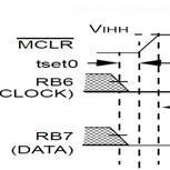
In the following text, I will be encouraging you to use your imagination and pretend you are in control of the clock and data, and will be sending commands and writing data one bit and one clock at a time, manually!
To accomplish this, you should imagine you have three bounce less switches named MCLR, Clock, and Data and the microcontroller setup on a solderless breadboard. RB7 would be a toggle switch, to select either HIGH or LOW for the data line.
RB6  RB7
RB7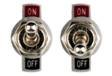
First we set MCLR, RB6 and RB7 to logic zero states. Once satisfied they are stable, the MCLR switch would be set to the 13volt state and locked there for the duration of our programming task. The zero to 13v transition should take mere microseconds or less.
You have just initiated a programming mode within the PIC microcontroller! Exactly like the diagram above.
Now that you have MCLR locked at 13volts, you will use the RB6 and RB7 switches for clock and data transitions as needed to enter our programming code and data.
The following paragraphs will show how the data gets into the PIC microcontroller one bit at a time, through the action of your manual control. That is, RB6 and RB7 Switches, your hands and your brain.
Second Method:
The second method, called Low Voltage ICSPTM or LVP for short, applies VDD to MCLR and uses the I/O pin RB3 to enter Programming mode. In this mode RB3 becomes dedicated to being the PGM pin and is not available as a GPIO pin.
When RB3 is driven to VDD from ground, the PIC16F87XA device enters Programming mode. See Table 1:1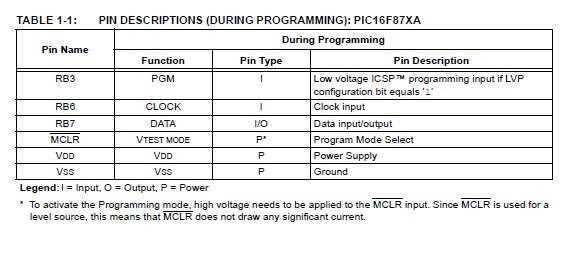
Because the timing diagrams in the document reflect the high voltage programming method, method 1, this article will ignore the low voltage method. I may do another article about method 2 in the future if this article works out.
We’re In Programming Mode….Now What?
Once you put the PIC controller in programming mode it is ready to respond to your input. But what the heck do you input?
Programming commands to the PIC microcontroller.
In each of the microcontrollers resides what’s known as microcode. It is internal programming completely hidden to the user but tells the controller chip how to operate. Each macro instruction, such as movwf (move w to a file) is performed by the microcode telling the controller circuitry what data to move into what register , how to set the status bits, and various other housekeeping chores. Everything is performed because the microcode controls the internal circuit pathways and registers.
So, it should not come as a surprise that when you raise the MCLR line to 13volts the controller goes into a very precise mode of operation that expects 12 commands from the user telling it what to do.
The controller needs to know what YOU want to do. Do you want to ‘load data for program memory’ or ‘begin an erase cycle’ for the whole chip. Whatever you tell the controller though, it will only be done using 12 commands listed in the following table.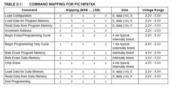
Each command will be discussed in turn to give a clear idea of what the controller expects in the way of commands and exactly what it does in response. I will even show how each command could be entered manually by our three bounce less switches (theoretically).
Later, when you have a fairly good idea of the commands available for your use, I will pull out the various programming algorithms from the Microchip PIC16F877A document and discuss the methods used by programming software.
Load Configuration
The PIC microcode will set the program counter (PC) to 2000h after receiving a six bit command (lsb first) of “000 000”. Upon recognition of the Load Configuration command The PIC microcode will expect 16 clock cycles on the RB6 pin. The first bit clocked will be a start bit on RB7, which is a zero or low by default.
Per Table 2-1 of the PIC programming commands, 14 bits of data representing the word to be programmed into the current address will be expected by the microcode.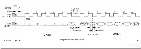
The final or 16th clock cycle on RB6 will clock in a zero as a STOP bit.
The above sequence could be entered manually by setting our RB7 toggle switch into the proper state for each clock cycle and then pushing RB6 closed and opened to generate the clock. (When closed, Rb6 causes the logic level to go HIGH. Upon release, the logic level returns to LOW.
We would start manually entering the command by setting RB7 to zero and clocking one clock with RB6.
Examination of the command table shows every bit of the Load Configuration command is zero, as is seen in the above timing diagram. Therefore all you need to do is cycle the RB6 switch six times to enter the command.
Just to remind ourselves what we are doing, I have reproduced the command entry portion of the timing diagram for the Load Configuration command, which we just manually entered.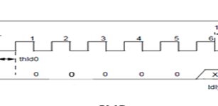 Microcode will accept the command and configure internally as necessary to receive fourteen data bits from the sixteen bits presented. That is probably why there needs to be a 1 microsecond delay (tdly2) minimum between entry of the command and entry of the 14 bits of data to be programmed into address 2000h.
Once the delay between command and data expires, microcode in the PIC controller will expect the fourteen data bits preceded and proceeded with a start/stop bit, respectively. We comply by setting the logic state of RB7 to zero for a start bit, and then clock it with RB6. Follow by setting the state of each individual bit of the 14 bit word (lsb first) with RB7 and clock the bit in with RB6. When the final (14th) bit of data is clocked in, we set RB7’s logic state to zero for the stop bit and clock it in with RB6.
Example. The word to be programmed is 2C53h. Remember, we send and receive data lsb first. We start with a zero for the start bit, clock it and follow with 11001010001101 and wrap it up with the final stop bit.
The Start bit The stop bit
Once again, just as a reminder, here is what we just did.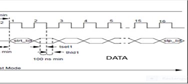
Congratulations, You just entered your first PIC Microcontroller Flash programming command and data content!
Configuration Memory
Since we are discussing the Load Configuration command, now would be a good time to discuss its memory locations, ID’s, etc.
A description of the memory mapping schemes of the program memory for normal operation and configuration mode operation is shown in Figure 2-1 of the programming specification document.
Figure 2-1 from the document is reproduced below for reference.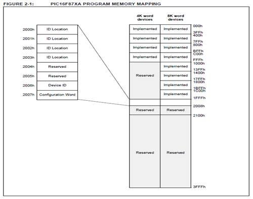
If we were to manually program the Configuration Memory fully, we would have to program four words of ID into addresses 2000h through 2003h. We would leave 2004h through 2005h alone, since those words are reserved. A Device ID would be burned into address 2006h, and finally 2007h would have the configuration word burned into it. That’s a lot of logic level clocking on our part!
You may have noticed that I haven’t mentioned how to get to the next address or what command to use after the very first Load Configuration command. Those topics will be discussed in future paragraphs. I’m sure you’re smart enough to guess what commands to use based on the table of commands. But leaving that for now…..
After the configuration memory is entered, the only way to get back to the user program memory is to exit the Program/Verify Test mode by taking MCLR low (VIL). That means we would put the MCLR switch into a logic low state. The PIC microcontroller would respond by going to RESET mode. For this reason, many programmers leave the Configuration section of memory for last in the programming task.
For reference, I also included section three configuration memory contents such as Device ID Word and Device Id Value. Look at Table 3-1 Device ID Value. It informs us that a 16F877A will have a Dev value of 00 1110 0010. Since I use the 877A often, it would be a good idea for me to remember that ID.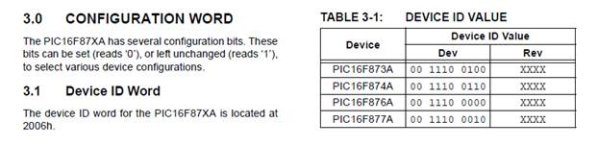 Register 3-1: Configuration Word Register is reproduced below. It shows us the various control bits we need to be concerned with, such as code protection or watch dog timer enable/disable.
If you have even a small amount of microcontroller programming experience, you’ll remember PIC programming software requires you to set the various states of these control bits prior to burning your hex code into the controller. If you wondered what was being done with that information, now you know. It is being burned into the Configuration Word Register, address 2007h.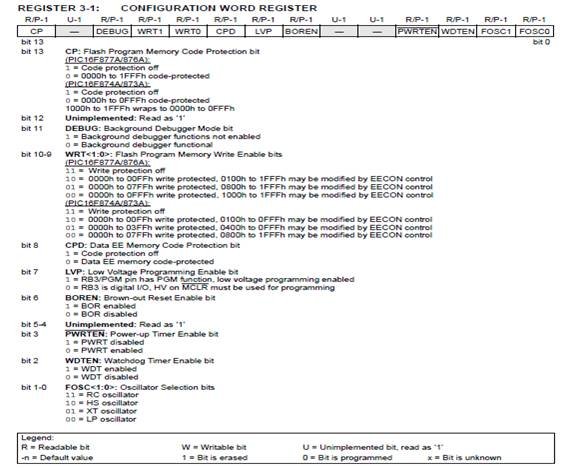
Load Data for Program Memory
After receiving this command, the chip will load one word (with 14 bits as a “data word”) to be programmed into user program memory when 16 cycles are applied. A timing diagram for this command is shown below.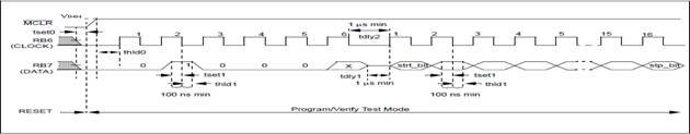 Study of timing diagram should reveal it is almost like the Load Configuration command. The only difference is the command word is 000010, instead of 000000, sent lsb first.
To execute this command you would clock in 0, toggle RB7 state to a 1 and clock it in, then toggle RB7 back to zero and clock four times. The PIC microcode will now configure internally to load the next sixteen bits you clock in. So you set RB7 to zero for the first start bit and clock it, then toggle the logic state for each bit on RB7 and clock it one at a time. Finally, you set the state of RB7 to zero for the sixteenth bit, the stop bit, and clock it in. That ends that command.
Load Data for Data Memory
After receiving this command, the chip will load in a 14-bit “data word” when 16 cycles are applied.
However, the data memory is only 8-bits wide, and thus, only the first 8 bits of data after the Start bit will be programmed into the data memory. It is still necessary to cycle the clock the full 16 cycles in order to allow the internal circuitry to reset properly. The data memory contains up to 256 bytes. If the device is
Code-protected, the data is read as all zeros. A timing diagram for this command is shown below. It can be seen in the timing diagram and verified with the command table that this command’s code is 000011 or 03 BCD. You will clock this command and following data in one bit at a time, just as you did with the previous commands. Remember the first start bit and the trailing stop bit, and entry is lsb first.
Read Data from Program Memory
After receiving this command, the chip will transmit data bits out of the program memory (user or configuration) currently accessed, starting with the second rising edge of the clock input. The RB7 pin will go into Output mode on the second rising clock edge, and it will revert back to Input mode (high-impedance) after the 16th rising edge. A timing diagram of this command is shown.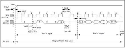 Manual entry of this command would be to repeat the clocking on RB6 and logic state changes on RB7 as with the previous commands. Remember data is read out lsb first.
Manual entry of the normal start bit clock, clock number 1, is all we need for this command, since there is no start or stop bit on a ‘read’ command. RB7’s logic state is not applicable and doesn’t matter, so you don’t have to set it to low.
On the rising edge of the second clock, the PIC controller microcode internally switches RB7 on the controller to ‘output’ mode. You no longer set the logic state for RB7. Instead, you will READ each bit presented to you by the controller on the RB7 pin. You must read and record RB7 output bit(0) through bit(13). After the rising edge of the sixteenth clock, the PIC microcode will revert the controller RB7 pin back to ‘input’ mode.
I’m sure by now you have a very good grasp of how to enter each command manually if you had to. From this point on I will include the timing diagram for each command but will leave the manual sequences up to you.
I don’t expect you will actually program a whole hex file into a PIC chip by hand, but I do expect you to mentally imagine the manual programming steps we covered in an attempt to burn the simplicity of programming into your mind.
My goal was for you to have the process of burning commands and data so ingrained into your head that you probably already feel you can imagine a fairly simple program with an Arduino or Raspberry Pi to perform your ‘manual’ switching. You are probably already thinking about how to write your own programmer.
Read Data from Data Memory
After receiving this command, the chip will transmit data bits out of the data memory, starting with the second rising edge of the clock input. The RB7 pin will go into Output mode on the second rising edge, and it will revert back to Input mode (high-impedance) after the 16th rising edge. As previously stated, the data memory is 8-bits wide, and therefore, only the first 8 bits that are output are actual data. A timing diagram for this command is shown in Figure 6-4. Remember the data read out will be lsb first. A 13h in memory would be read as 1100 1000 xxxx xxb. If you had some kind of hardware reading the data, you would have to ensure its programming arranged the bits correctly so 13h was correctly recovered. Also, like before when we read data from program memory, the RB7 pin transitions from ‘input mode’ to ‘output mode’ on the second clock cycle rising edge, and there is no start bit necessary for the first clock cycle. Finally, on the sixteenth clock rising edge the microcode switches the RB7 pin back to ‘input mode’.
Increment Address
The PC is incremented when this command is received. A timing diagram of this command is shown.
Notice there is no data written or read after receipt of the command. The PIC microcode simply increments the PC to the next address and then assumes the next event it should wait for is a new command.
Now you know how we jump to the next address when finished with a command. This is the tool you’ve been waiting for. Very soon now we will go over programming algorithms suggested by Microchip which will tie all these (Manual) processes together for efficient programming. But first, Erase commands need to be discussed.
Begin Erase/Program Cycle
Eight locations must be loaded before every ‘Begin Erase/Programming’ command. After this command is received and decoded, eight words of program memory will be erased and programmed with the values contained in the program data latches. The PC address will decode which eight words are programmed.
The lower three bits of the PC are ignored, so if the PC points to address 003h, then all eight locations from 000h to 007h are written. An internal timing mechanism executes an erase before write. The user must allow the combined time for erase and programming, as specified in the electrical specs, for programming to complete. No ‘End Programming’ command is required.
1. If the address is pointing to user memory, the user memory alone will be affected.
2. If the address is pointing to the physically implemented test memory (2000h – 201Fh), test memory
will be written. The configuration word will not be written unless the address is specifically pointing to 2007h. This command can be used to perform programming over the entire VDD range of the device.
A timing diagram for this command is shown.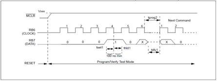
Begin Programming Only
This command is similar to the ‘Erase/Programming Cycle’ command, except that a word erase is not
done, and the internal timer is not used. Programming of program and data memory will begin after this command is received and decoded. The user must allow the time for programming, as specified in the electrical specs, for programming to complete. An ‘End Programming’ command is required.
The internal timer is not used for this command, so the ‘End Programming’ command must be used to stop programming.
1. If the address is pointing to user memory, the user memory alone will be affected.
2. If the address is pointing to the physically implemented test memory (2000h – 201Fh), the test
memory will be written. The configuration word will not be written unless the address is specifically pointing to 2007h. A timing diagram for this command is shown.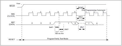
Erasing Program and Data Memory
Depending on the state of the code protection bits, program and data memory will be erased using different methods. The first two commands are used when both program and data memories are not code-protected. The third command is used when either memory is code-protected, or if you want to also erase the fuse locations, including the code-protect bits. A device programmer should determine the state of the code protection bits and then apply the proper command to erase the desired memory.
ERASING NON-CODE PROTECTED PROGRAM AND DATA MEMORY
When both program and data memories are not code-protected, they must be individually erased using the following commands. The only way that both memories are erased using a single command is if code protection is enabled for one of the memories. These commands do not erase the configuration word or ID
locations.
Bulk Erase Program Memory
When this command is performed, and is followed by a ‘Begin Erase/Programming’ command, the entire
program memory will be erased. If the address is pointing to user memory, only the user memory will be erased.
If the address is pointing to the test program memory (2000h – 201Fh), then both the user memory and the test memory will be erased. The configuration word will not be erased, even if the address is pointing to location 2007h. Previously, a load data with 0FFh command was recommended before any Bulk Erase. On these devices, this will not be required.
The Bulk Erase command is disabled when the CP bit is programmed to ‘0’ enabling code-protect. A timing diagram for this command is shown.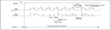
Bulk Erase Data Memory
When this command is performed, and is followed by a ‘Begin Erase/Programming’ command, the entire data memory will be erased. The Bulk Erase Data command is disabled when the CPD bit is programmed to ‘0’ enabling protected data memory. A timing diagram for this command is shown.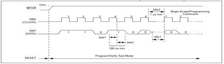
Chip Erase
This command, when performed, will erase the program memory, EE data memory, and all of the fuse
locations, including the code protection bits. All on-chip Flash and EEPROM memory is erased,
regardless of the address contained in the PC. When a Chip Erase command is issued and the PC
points to (0000h – 1FFFh), the configuration word and the user program memory will be erased, but not the test row (see Section 2.5.2.1 of 16F87XA Flash Memory Programming Specification) and two headings down for additional Chip Erase information.
Chip Erase can also be used to erase code-protected memory, as described in Section 2.5.2 of 16F87XA Flash Memory Programming Specification. This command will also erase the code-protect and code-protect data fuses if they are programmed. This is the only command that allows a user to erase the code-protect fuses.
The Chip Erase is internally self-timed to ensure that all program and data memory is erased before the code-protect bits are erased. A timing diagram for this command is shown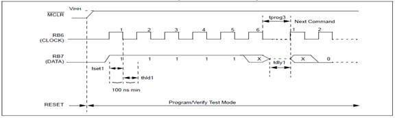
ERASING CODE PROTECTED MEMORY
For the PIC16F87XA devices, once code protection is enabled, all protected program and data memory locations read all ‘0’s and further programming is disabled. The ID locations and configuration word read out unscrambled and can be reprogrammed normally. The only command to erase a code-protected PIC16F87XA device is the Chip Erase. This erases program memory, data memory, configuration bits and ID locations.
Since all data within the program and data memory will be erased when this command is executed, the security of the data or code is not compromised.
Chip Erase (additional information)
This command, when performed, will erase the program memory, data EEPROM, and all of the fuse locations, including the code protection bits, code-protect fuses, and code-protect data fuses. All on-chip Flash and EEPROM memory is erased, regardless of the address contained in the PC.
If the PC points to user memory, the test row (2000h through 201Fh) is not erased with a Chip Erase command, except for the configuration word (at 2007h). If the test row is to be completely erased, the address in the PC must point to configuration memory. When the PC points to 2000h – 201Fh, the configuration word, test program memory, and the user program memory will all be erased with a Chip Erase command. This allows the user to erase all program and configuration content, including the code-protect bits, without compromising the user ID bits (2000h through 2004h), or any pass codes stored in the test row.
Let us step back now to a wider view of programming operations and Re-enter programming mode once again, so we can discuss more topics that need covered.
Program/Verify Mode
The Program/Verify mode is entered by holding pins RB6 and RB7 low, while raising MCLR pin from VIL to VIHH (high voltage). In this mode, the state of the RB3 pin does not affect programming. Once in this mode, the user program memory and the configuration memory can be accessed and programmed in serial fashion. The mode of operation is serial, and the memory accessed is the user program memory. RB6 and RB7 are Schmitt Trigger inputs in this mode.
The sequence that enters the device into the Programming/Verify mode places all other logic into the RESET state (the MCLR pin was initially at VIL). This means all I/O are in the RESET state (high impedance inputs). A device RESET will clear the PC and set the address to ‘0’. The ‘Increment Address’ command will increment the PC. The ‘Load Configuration’ command will set the PC to 2000h. The available commands are shown in Table 2-1.
Programming Eight Program Memory Words at a Time.
The normal sequence for programming eight program memory words at a time is as follows:
1. Load a word at the current program memory address using the ‘Load Data’ command.
2. Issue an ‘Increment Address’ command.
3. Load a word at the current program memory address using the ‘Load Data’ command.
4. Repeat Step 2 and Step 3 six times.
5. Issue a ‘Begin Programming’ command to begin programming.
6. Wait tprog (about 1 ms).
7. Issue an ‘End Programming’ command.
8. Increment to the next address.
9. Repeat this sequence as required to write program and configuration memory.
The sequence above is shown as a flow diagram below.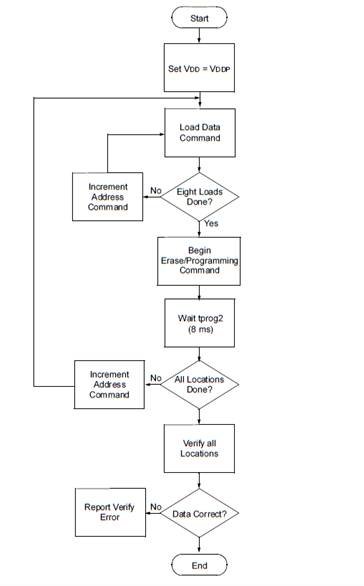
Programming One Program Memory Word at a Time.
The alternative sequence for programming one program memory word at a time is as follows:
1. Set a word for the current memory location using the ‘Load Data’ command.
2. Issue a ‘Begin Programming Only’ command to begin programming.
3. Wait tprog.
4. Issue an ‘End Programming’ command.
5. Increment to the next address.
6. Repeat this alternative sequence as required to write program and configuration memory.
The address and program counter are reset to 0000h by resetting the device (taking MCLR below VIL) and re-entering Programming mode. Program and configuration memory may then be read or verified using the ‘Read Data’ and ‘Increment Address’ commands.
Out of the Frying Pan and Into the Fire.
Ok, we know how to program a PIC microcontroller now, but it is all theory. We pushed buttons in our imagination to program imaginary commands and data into an imaginary controller one command at a time. What we need to do now is back out with our focus, from individual commands, bits and clocks to a wider scope of programming operation. Where does the data of the 14 bit words burned into the PIC controllers memory come from? How can we know ahead of time what that data will consist of?
Can we interpret the data source by sight alone?
The Answer as you most likely already know, is the .hex file. There are several different varieties of hex files, but the most common, and the one utilized in 99.9% of programmers used with the PIC microcontrollers, is the Intel Hex Format. An Intel hex file of one of my own programs is reproduced here as an example. We will examine it later in greater detail.
:100000000A128A11052800000900831691010730A1
:1000100083129900FF308316850087018312051C27
:100020001A280710851A07148710051A8714071154
:0E00300085190715051C1D281A280F281E28E3
:02400E00C431BB
:00000001FF
The Intel HEX file is an ASCII text file with lines of text that follow the Intel HEX file format. Each line in an Intel HEX file contains one HEX record. The First line of the above hex file is one hex record. It is shown in stand alone fashion here.
:100000000A128A11052800000900831691010730A1
These records are made up of hexadecimal numbers that represent machine language code and/or constant data. Intel HEX files are often used to transfer the program and data that would be stored in a ROM or EPROM. Most EPROM programmers or emulators can use Intel HEX files.
Record Format
An Intel HEX file is composed of any number of HEX records. Each record is made up of five fields that are arranged in the following format:
:llaaaatt[dd…]cc
Each group of letters corresponds to a different field, and each letter represents a single hexadecimal digit. Each field is composed of at least two hexadecimal digits-which make up a byte-as described below:
: is the colon that starts every Intel HEX record.
ll is the record-length field that represents the number of data bytes (dd) in the record.
aaaa is the address field that represents the starting address for subsequent data in the record.
tt is the field that represents the HEX record type, which may be one of the following:
00 – data record
01 – end-of-file record
02 – extended segment address record
04 – extended linear address record
05 – start linear address record (MDK-ARM only)
dd is a data field that represents one byte of data. A record may have multiple data bytes. The number of data bytes in the record must match the number specified by the ll field.
cc is the checksum field that represents the checksum of the record. The checksum is calculated by summing the values of all hexadecimal digit pairs in the record modulo 256 and taking the two’s complement.
Putting these definitions into practice with the above hex file example, starting with line one, we have:
:llaaaatt[dd…]cc (the Intel Hex file Format)
Colons (:) precede each line or hex record.
: 100000000A128A11052800000900831691010730A1
: 1000100083129900FF308316850087018312051C27
: 100020001A280710851A07148710051A8714071154
: 0E00300085190715051C1D281A280F281E28E3
: 02400E00C431BB
: 00000001FF
ll is the record-length field that represents the number of data bytes (dd) in the record.
: 10 0000000A128A11052800000900831691010730A1
: 10 00100083129900FF308316850087018312051C27
: 10 0020001A280710851A07148710051A8714071154
: 0E 00300085190715051C1D281A280F281E28E3
: 02 400E00C431BB
: 00 000001FF
In the example, the first three lines (hex records) is 10h, or 16 decimal, telling us the
record holds 16 bytes of data content to be programmed into memory. In the fourth
record, there are 0Eh data bytes or 14 decimal bytes of content. The fifth record, and
last line with actual data content, contains two bytes of data which in this case is the
configuration word to be written in address 2007.
The last line consists of End of Record type and Record checksum, so the number
data bytes it holds is zero. The last line will be discussed again when we get to record
type.
aaaa is the address field that represents the starting address for subsequent data in the record.
: 10 0000 000A128A11052800000900831691010730A1
: 10 0010 0083129900FF308316850087018312051C27
: 10 0020 001A280710851A07148710051A8714071154
: 0E 0030 0085190715051C1D281A280F281E28E3
: 02 400E 00C431BB
: 00 0000 01FF
It can be seen that the first record contents will start at location 0000. The second at 0010. The third and fourth records’ contents will be stored starting at locations 0020 and 0030, respectively.
Then, there is the fifth record address of 400E.
I just happen to know that this is the configuration WORD address of 2007 because the configuration word for this program is 31C4, which can be seen in the data field of that record as C4 31.
Remember, each program instruction is 14 bits residing in 16 bit words. Since there are two bytes to each word, a word address of 2007h would be twice as many bytes. Hence 400E is the physical address in bytes.
Finally we have the last record. It says there are no data bytes in the record and no address. Its record TYPE is 01, which is an ‘end of record’ type according to convention as listed above. The checksum for the record is FF.
There you have it! Now you can confidently say you know how programmers get your programs into a PIC microcontroller, and how the hex file is used to do it. I’ll bet the only frustration you experience now is what to do with all this new found learning. You probably have quite a few ideas for stand-alone programmers, or using an Arduino as a PIC programmer, or even a Raspberry Pi. The possibilities are endless. Myself, I am working on converting an old MeLabs parallel port Epic programmer into a stand-alone programmer which responds to commands and data I send to it via push buttons, toggle switches, and, of course, a specially programmed PIC microcontroller. What could be more natural?
[box type=”note” head=”Article Written By”]Thomas R. Hackwelder – An Embedded Expert[/box]