Summary of The Zeta minimal Z80 toggle-switch computer
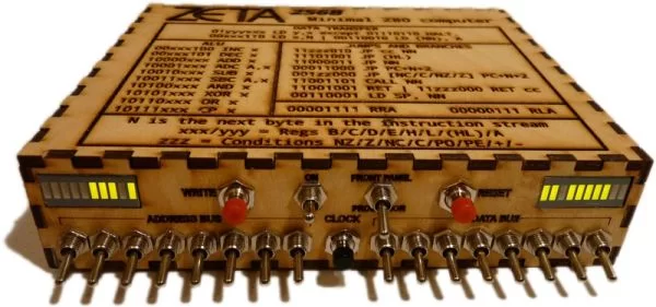
The Zeta is a minimal Z80 toggle-switch computer featuring a Zilog Z80 microprocessor, 256 bytes of RAM, and a front panel for direct bus interaction. It lacks standard interfaces, relying on switches to set addresses and data. The design utilizes stripboard layouts generated in Inkscape, with plans for future KiCad diagrams. While it executes algorithms like Euclid's, the current documentation notes missing details regarding track cuts and voltage regulator components.
Parts used in the Zeta:
- Zilog Z80 microprocessor
- 256 bytes of RAM
- Front panel
- Address buses
- Data buses
- Write button
- !BUSREQ pin
- !BUSACK pin
- SN74LVC245AN chips (input buffers)
- Voltage regulators
The Zeta is a minimal Z80 toggle-switch computer. It has a Zilog Z80 microprocessor, 256 bytes of RAM and the only interface is the front panel which directly sets and reads the address and data buses.
There is a video of it executing Euclid’s algorithm:
https://www.youtube.com/watch?v=0GmY_UrbXnA
At the moment, there is only one real source file in this repository, an Inkscape-produced SVG which contains the stripboard layout and lasercut paths along with the image for the box top. In the future I’ll try to add a KiCad circuit diagram. This file doesn’t preview well in github because there are some very thin and zero-width lines – turn on outline mode (View -> Display mode -> Outline) in Inkscape to view it.
Note that this isn’t a foolproof guide to building a replica – there are several parts not recorded yet, such as where to cut the track on the stripboard, and some extra components for the voltage regulators.
There are some errata in the current source – please see the issues section for details.
Why is your circuit diagram in SVG?
Because of the number of DIP chips in this project, it suits stripboard well, and I haven’t found a good program for designing stripboard layouts yet. Fritzing supports small stripboard, but has performance problems when you use a layout as big as this one.
How does it work?
The Z80 has two pins called !BUSREQ and !BUSACK. !BUSREQ is an input, normally high (5V), which means the Z80 is in control of the address and data buses, except when RD is high which means the RAM chip can control the data bus. The “Front Panel/Processor” switch on the front panel pulls !BUSREQ to 0V when “Front Panel” is selected. After a few clock cycles, the Z80 will then drop the output !BUSACK. This is connected to the output enable pins of the two input buffers (the SN74LVC245AN chips). The switch positions are then driven onto the buses, and you can enter data into the RAM using the write button.
For more detail: The Zeta minimal Z80 toggle-switch computer
- What interface does the Zeta use?
The only interface is the front panel which directly sets and reads the address and data buses. - How does the switch control the buses?
The Front Panel/Processor switch pulls !BUSREQ to 0V when Front Panel is selected, allowing switch positions to drive the buses. - Why is the circuit diagram in SVG format?
SVG suits the project because of the number of DIP chips and the lack of good programs for designing large stripboard layouts. - Can Fritzing be used for this layout?
Fritzing supports small stripboard but has performance problems when using a layout as big as this one. - Is there a video of the computer executing an algorithm?
Yes, there is a video of it executing Euclid's algorithm available on YouTube. - Does the article provide a complete guide for building a replica?
No, it is not a foolproof guide because several parts are not recorded yet, such as where to cut the track on the stripboard. - What components are currently missing from the documentation?
Extra components for the voltage regulators and specific track cuts on the stripboard are not recorded yet. - How does the Z80 release control of the data bus?
The Z80 drops the output !BUSACK after clock cycles, enabling the input buffers so the RAM chip can control the data bus when RD is high.