Summary of Simple circuit lets you characterize JFETs
This article describes a simple test circuit that quickly measures a JFET’s pinch-off voltage (VP) and zero-bias drain current (IDSS) to accommodate device-to-device parameter variation. Using a switchable op-amp buffer/gain stage and resistor network, the circuit reads VP directly and reads IDSS as a voltage across a 100 Ω apparent resistance (gain-of-10). It supports N- or P-channel devices, includes stability and protection components, and helps select matched or optimal discrete JFETs.
Parts used in the JFET characterization tool:
- JFET DUT (N-channel or P-channel)
- Op amp (unity buffer / gain-of-10)
- R1 (allows microamp drain current in pinch-off mode)
- R2 (10 Ω source-to-ground resistor in IDSS mode)
- R3 (feedback resistor for unity gain)
- R4 (part of feedback divider for gain-of-10)
- R5 (part of feedback divider for gain-of-10)
- R6 (isolates op-amp feedback from voltmeter capacitance)
- R7 (short-protection resistor)
- Apparent 100 Ω measurement resistance (implemented as circuit reading corresponds to IDSS × 100 Ω)
- C1 (bypass capacitor to suppress high-frequency oscillation)
- Switch S1 (selects N- or P-channel polarity)
- Switch S2 (selects pinch-off-voltage or zero-bias-drain-current mode)
- External voltmeter (reads pinch-off voltage or scaled IDSS)
- Test leads and clips (to connect DUT)
When working with discrete JFETs, designers may need to accommodate a large variation in device parameters for a given transistor type. A square-law equation is usually used as an approximate model for the drain-current characteristic of the JFET: ID=β(VGS−VP)2, where ID is the drain current, VGS is the gate-to-source voltage, β is the transconductance parameter, and VP is the gate pinch-off voltage. With this approximation, the following equation yields the zero-bias drain current at a gate-to-source voltage of 0V: IDSS=βVP 2, where IDSS is the zero-bias drain current.
Although you can design around a certain amount of device variation for a mass-produced circuit, you sometimes need a tool to quickly characterize an assortment of discrete devices. This tool allows you to select a device that will optimize one circuit or perhaps to find a pair of devices with parameters that match reasonably well.
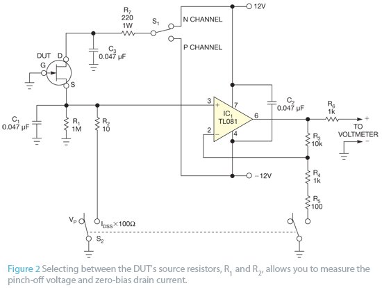
Figure 2 shows a simple test circuit for this purpose. Although the figure shows the JFET as an N-channel device, the JFET DUT (device under test) may be of either polarity, as selected by switch S1. An external voltmeter connects to the terminals on the right. Switch S2 selects two distinct measurement modes—one for the pinch-off voltage and another for the zero-bias drain current. In the pinch-off-voltage mode, the external voltmeter directly reads the pinch-off voltage; in the zero-bias-drain-current mode, the measured voltage is the zero-bias drain current across an apparent resistance of 100Ω.
With S2 in the pinch-off-voltage mode, R1 allows a few microamps of drain current to flow in the JFET under test, and the source voltage is a close approximation of the negative of the pinch-off voltage. The op amp acts as a unity-gain buffer, with negative feedback through R3, so you can directly read the negative of the pinch-off voltage with the external voltmeter.
In the zero-bias-drain-current mode, however, the resistance from JFET source to ground is only 10Ω, so the drain current is a close approximation of the zero-bias drain current. The op amp’s feedback also switches to a gain-of-10 configuration, with the inclusion of R4 and R5 in the feedback-voltage divider. This gain allows the voltmeter to easily read the small voltage across R2, with the resulting reading being the zero-bias drain current times 100Ω. For example, if the voltmeter reads 1V, this voltage corresponds to a zero-bias drain current of 10 mA.
By clipping in samples from a collection of JFETs and throwing a switch, you can very quickly find the two parameters that determine where each JFET’s characteristic falls in the range that Figure 1 illustrates and select devices to optimize circuit performance.
For more detail: Simple circuit lets you characterize JFETs
- How does the circuit measure pinch-off voltage?
With S2 in pinch-off mode, R1 provides a few microamps of drain current and the op amp in unity-buffer configuration lets the voltmeter read the negative of the pinch-off voltage at the source. - How does the circuit measure zero-bias drain current IDSS?
With S2 in IDSS mode, the source-to-ground resistance is about 10 Ω so drain current approximates IDSS; the op amp is switched to a gain-of-10 so the voltmeter reads IDSS times 100 Ω. - Can the circuit test both N-channel and P-channel JFETs?
Yes; switch S1 selects device polarity, yielding positive readings for N-channel and negative readings for P-channel devices. - Why is C1 included in the circuit?
C1 is added to suppress any tendency for high-frequency oscillation caused by test leads and clips with parasitic inductance. - What is the purpose of R6?
R6 isolates the op amp feedback loop from any parasitic capacitance in the voltmeter and its leads to preserve loop stability. - What does R7 protect against?
R7 provides protection against accidental shorts. - How is the voltmeter reading related to IDSS numerically?
The voltmeter reading equals IDSS multiplied by 100 Ω, so 1 V corresponds to IDSS of 10 mA. - Can R4 and R5 be replaced by a single resistor?
You can replace R4 and R5 with one 1.1-kΩ resistor, though discrete resistor values shown are more commonly available. - Why use this test circuit with samples of JFETs?
To quickly find VP and IDSS for each JFET so you can select devices that optimize circuit performance or match parameters.