
Summary of PICADC – a free, PIC based “intelligent” A/D converter using PIC16F84
The PICADC is a simple, low-cost 12-bit analog-to-digital converter with eight channels and four digital inputs. It connects to a PC via RS232, allowing programmable sampling sequences and frequencies up to approximately 3kHz per channel. The device operates on a voltage range of -2.5V to 2.5V and utilizes a PIC16F84 microcontroller paired with a MAX190 or MAX191 ADC chip. The design features a single-sided PCB suitable for home construction, though some components like tantalum capacitors require careful polarity handling.
Parts used in the PICADC:
- PIC16F84 (or 166C84) microcontroller
- MAX190 (or MAX191) ADC
- Single-sided printed circuit board (PCB)
- Tantalum capacitors (4u7)
- RS232 serial interface components
- Resistors R18 and R21 (optional)
- J2 connector for RESET pin connection
- MAX232 level converter (for non-optoisolated setups)
This is an old design. Some of the components may be difficult to buy. If you would like to build an even better and cheaper A/D converter, take a look at the new PICADC3 design. The PICADC is a simple 12-bit, 8-channel analog to digital converter (with 4 additional digital inputs), which may be connected to the PC through the serial interface (RS232).
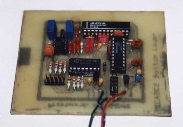
The sequence of sampled channels, and sampling frequence are programmed by the PC.
The maximal sampling frequency is limited by the data transmission rate, and at 115200 baud is equal to ca. 3kHz for 1 channel without digital inputs, and to ca. 500 Hz for 8 channel with digital inputs.
The analog input voltage range is -2.5V to 2.5V.
The digital inputs may be used for recording additional digital signals, eg. the time code used to synchronize the recorded data with other events.
The PICADC is based on PIC16F84 (or 166C84) microcontroller, and MAX190 (or MAX191) ADC.
The device is mounted on a small single-sided printed board, easy to prepare even at home, shown in the figure below (and available in the Easytrax for DOS format). There also printouts of the bottom layer, and top overlay available in the PDF format
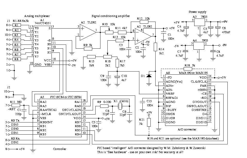
The schematic diagram of PICADC is shown in the picture below, and is also available in the PDF format.
The R18 and R21 resistors are not mounted on my board. The R18 may be used to change the compensation mode of internal voltage reference in MAX190/191 (see the MAX190/191 data sheet), and R21 may be used to pull up the data line, when MAX190’s DOUT is in high impedance state.
The 4u7 capacitors (C4, C5, C7, C8, C10) should be tantalium capacitors (watch the polarity, when mounting them!).
The PICADC was intended to be a part of an optoisolated data acquisition system. Therefore its PCB does not contain the RESET circuitry and RS level converters, which should be connected through the transoptors. However usually the RESET switch is not needed and you can connect the ~RST pin (7) in the J2 connector to the +5V (J2 pin 8). If the optoisolation is not needed, you can use the MAX232 as the level converter, or simple circuits shown in the figure below:
For more detail: PICADC – a free, PIC based “intelligent” A/D converter using PIC16F84
-
What is the maximum sampling frequency for one channel?
The maximal sampling frequency is approximately 3kHz for 1 channel without digital inputs at 115200 baud. -
Can I use this project to record time codes?
Yes, the 4 additional digital inputs may be used for recording additional digital signals like time codes. -
What type of capacitors should be used for C4, C5, C7, C8, and C10?
These positions require 4u7 tantalum capacitors, and users must watch the polarity when mounting them. -
Does the PCB include built-in reset circuitry?
No, the PCB does not contain RESET circuitry because it was intended for an optoisolated system. -
How do I handle the ~RST pin if optoisolation is not needed?
You can connect the ~RST pin (pin 7) in the J2 connector to the +5V (J2 pin 8). -
What is the analog input voltage range for this device?
The analog input voltage range is specified as -2.5V to 2.5V. -
Is there a better alternative to this old design mentioned?
Yes, the article suggests looking at the new PICADC3 design for an even better and cheaper A/D converter. -
Where can I find the schematic and PCB layouts?
Schematics are available in PDF format, and the PCB layout is available in Easytrax for DOS format.
