An alliance led by IBM Research, together with New York academic institution SUNY Polytech and with Samsung and GlobalFoundries, has produced 7nm (nanometer) node test chips with functioning transistors.
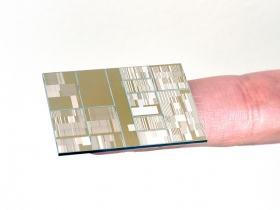
Continuing semiconductor scaling down to feature sizes of 7 nm is expected to yield further gains in performance, and lower power levels, but in IBM’s words, “[its] researchers had to bypass conventional semiconductor manufacturing approaches”. The finFET-style transistors in the demonstrator were constructed with silicon-germanium (SiGe) channels, and the lithography that defined them employed Extreme Ultraviolet (EUV) technology, “at multiple levels”. [That is, the use of EUV was not reserved for definition of a single critical part of the transistor structure.]
For more detail: News about Ibm Shows Working Devices Fabricated At 7nm Node