The Microchip PIC32 is a family of complex and powerful microcontrollers that can be purchased for less than $10 in quantities of one. This microcontroller offers many peripherals useful for mechatronics purposes, such as several channels for analog-to-digital conversion, digital I/O, synchronous and asynchronous serial communication, pulse width modulation, etc. For our purposes, the primary advantages of the 32-bit PICs over the 8-bit PICs we have used (and will continue to use) are that they are faster (max clock rate of 80 MHz compared to 40 MHz), have more peripherals available, offer more program memory (flash) and data memory (RAM), and have significantly more computational horsepower due to the 32-bit address and data buses and single-cycle multiply for 32-bit math. The primary disadvantages are that they come only in surface mount packages, making them harder to work with for fast prototyping compared to the DIP (dual-inline packages) 8-bit PICs that can be plugged into a breadboard; and they must be powered by 2.3-3.6 V, unlike the 5 V of DIP 8-bit PICs and some DIP chips we would like to interface with. (Of course surface mount and lower operating voltages are vastly superior for commercial embedded products, and we will find ways to work around the disadvantages mentioned.)
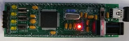
Particular numbers referenced on this page refer to the PIC32MX460F512L chip, which is the PIC32 used on the NU32 board. (You may wish to compare the capabilities of our PIC to others on the Microchip PIC32 parametric table.) The NU32 development board is shown at right. The NU32 board was designed by Andy Long to easily plug into a standard prototyping breadboard (DIP profile), allowing easy prototyping with the PIC32. The NU32 board also has a voltage regulator, a USB connector, and a few LEDs and switches to allow you to get up and running quickly with only the assembled NU32 board, a USB cable, and a PC with free software downloaded from Microchip (once a “bootloader” is installed on the PIC to allow you to program it from your PC). See the getting started page. The NU32 board was created with inspiration from the UBW32 board. We wanted a board that was a little bit smaller, so we sacrificed some pins we thought unnecessary for the majority of mechatronics projects. We also wanted a board that gave students some experience soldering non-surface-mount components.
The purpose of this page is to provide a brief overview of PIC32 and NU32 hardware and programming for the beginner. Microchip provides many reference manuals, data sheets, application notes, and sample software, and there are many other helpful web resources to take you further.
PIC32 Hardware Overview
Our PIC32MX460F512L features a max clock frequency of 80 MHz, 512K program memory (flash), 32K data memory (RAM), multiple interrupt sources and handling routines, 16 10-bit analog-to-digital input channels, many digital I/O channels (with outputs that can be configured for open-drain), USB 2.0, two I2C and two SPI synchronous serial communication modules, two UARTs for RS-232 or RS-485 asynchronous serial communication, five 16-bit counter/timers (configurable to give two 32-bit timers), five pulse-width modulation outputs, and a number of pins that can generate interrupts based on external signals, among other features. This PIC has 100 pins, many (but not all) of which are used or broken out by the NU32 board.
To cram this much functionality into 100 pins, many of the pins serve multiple functions. For example, pin 20 can serve as a comparator input, an analog input, a change notification input which can generate an interrupt when the pin changes state, or a digital input or output. Which function a particular pin serves is determined by “Special Function Registers” (SFRs) that contain configuration bits specifying the desired use of the pin. Typically your program sets these configuration bits at the beginning of execution, and the functions of the pins are fixed while your program runs. (It is possible, though rarely needed, to change the configuration bits and change the function of pins on the fly.)
A figure showing the pin-out of the PIC32MX4XX is shown at right. Shaded pins tolerate up to 5.5 V as inputs, and pins that are “checked” are brought out to the pins of the NU32 board, described below. Click on the image for higher resolution.
Below the different pin functions are briefly summarized. The most important functions for ME 333 are indicated in bold. To learn more about these functions, you can consult the data sheet, but for the most part you will learn how to use these functions by modifying sample programs. See also the Further Reading section at the bottom of the page.
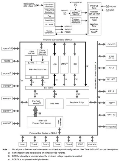
The figure at right is a block diagram of the architecture of the PIC32. The CPU (which operates at 1.8V, provided by a voltage regulator internal to the PIC32 as it’s used on the NU32 board) interfaces with data memory (RAM) and the program flash memory (along with USB, a direct memory access controller, and in-circuit debugger and JTAG interfaces that can be used for programming and debugging purposes). It also interfaces with peripherals, which are what make microcontrollers useful for embedded control. These peripherals consist of PORTA … PORTG, which are digital I/O ports; five 16-bit counters (can create 32-bit counters by chaining) that can be used for a variety of counting operations, and timing operations by counting clock ticks; analog-to-digital converter (ADC) multiplexed to 16 input pins; a real-time clock and calendar (RTCC) that can maintain accurate year-month-day-time; two comparators that compare which of two inputs has a higher voltage; UARTs for asynchronous serial communication (e.g., RS-232, RS-485); a “parallel master port” (PMP) for parallel communication; two I2C and two SPI synchronous serial communication modules; five pins for “input capture”, where interrupts can be triggered by rising or falling edges; five pins for pulse-width modulation (or “output compare”); and 22 change notification pins to generate interrupts when signals change.
Note that the peripherals are on two different buses: one is a bus clocked by the system clock SYSCLK, and the other is clocked by the peripheral bus clock PBCLK. These may be the same frequency, or PBCLK may be a lower frequency, depending on how you set clock configuration bits. The top of the figure shows the timing generation, which uses either an external crystal or timing circuit (for more accurate timing), or an internal circuit, to create SYSCLK, PBCLK, and 48 MHz USBCLK (which is used for USB communication). The NU32 board uses an external 8 MHz crystal oscillator to generate a SYSCLK and PBCLK of 80 MHz using a phase-locked loop (PLL) to multiply the frequency. This is set by the software, as discussed below, not by the physical design of the board. If the Watchdog Timer is used by your program, your program must periodically reset the timer counter. Otherwise the PIC will reset. This is a way to have the PIC recover and restart if your program has entered an unexpected state.
The CPU also interfaces with a “pre-fetch (cache) module.” This module fetches blocks of program instructions from flash program memory in advance of their use by the CPU, to try to limit delays due to relatively slow flash memory.
NU32 Development Board Overview
Here is a schematic of the NU32 development board, showing how the PIC32MX460F512L is used on the board, and showing which pins are made available to the user. The board layout is shown at right as and can be clicked on to view a high resolution image. It is also available as a pdf file. This excel spreadsheet details which of the PIC32 pins are used on the board, which are connected to pins available to the user, and which are not used. The mapping from the 58 pins on the NU32 board to pins on the PIC32 is also shown in the figure below. In total, 52 PIC pins are carried to the NU32 board pins.
The 27 PIC32 pins that are used on the board and not carried out to the board edge are 3, used for the USER switch; 30 and 31, the positive and negative references for the ADC (set to 3.3V and ground on the board); 51, 54, 55, 56, and 57, used for USB communication; 63 and 64, used for the oscillator; 85 and 86, related to the use of the PIC32’s internal 1.8V regulator for the core; 93, 94, 98, and 99, which are used as digital outputs for the four LEDs on the board; and 100, used for the PRG switch. Also, VDD pins 2, 16, 37, 46, and 62 are connected to +3.3V on the board, and VSS pins 15, 36, 45, 65, and 75 are connected to ground.
The 21 PIC32 pins that are not connected at all are 1 (dig I/O); 4 and 5 (parallel port and dig I/O); 17, 38, 60, and 61 (JTAG debugging and dig I/O); 79, 80, 82, 83, 84, 87, 88, 89, and 90 (primarily parallel port); and 91, 92, 95, 96, and 97 (trace debugging).
Options for powering the NU32 board:
- Plug a USB cable in and slide the power switch to USB power (toward the outside of the board). The USB cable provides 5V power, with a typical current supply of around 500 mA.
- Plug a power jack (2.5 mm ID, 5.5 mm OD, center positive) into the barrel connector on the board and slide the power switch to side labeled ‘EXT’ (toward the inside of the board). There are two options for this power jack.
- Any regulated or unregulated voltage 5V or greater. In this case, you must solder a 5V voltage regulator into the pins lableled LM2940. One possibility that will fit in the designated space is the LM2940 in the TO-220 package. This is a low-dropout regulator that can source up to 1 A. (In this case, “low dropout” means that your input voltage only has to be at least 0.5 or 1V above 5V; some cheaper regulators require that the input voltage be 2V above 5V.) The back of the LM2940 should be to the outside of the board.
- 5V regulated power. In this case, you do not need a regulator, but you must solder a jumper between the first and third pins of the voltage regulator pins labeled LM2940.
- If you do not have a connector that plugs into the barrel connector, you can solder wires into the holes labeled V+ and GND on the outer edge of the board, right after pin 58. Connect these wires to your power supply. These wires now replace the jack connector in the bullet above. See the rest of the description there.
NOT RECOMMENDED: If none of the power connections above are available, it is possible to power the board by providing 5V at pins 1 or 58 of the NU32 board. These pins are are connected to the USB 5V when the power switch is in the USB position, and they are connected to the output of the 5V regulator when the power switch is in the EXT position. This method should be avoided, to prevent accidental wiring that could damage the PIC.
Note on using the 3.3V and 5V output pins:
If the NU32 is powered by a USB cable, typically such a connection can only provide about 500 mA total. Take this into account when you decide how much current to try to draw from these pins. Even if the NU32 board is powered by a higher-current supply, such as a battery or a wall-powered adapter brick, keep in mind that the onboard 3.3V regulator can only source approximately 950 mA max. You should not try to draw more than, say, half that. Also, if your supply is unregulated and you are using a 5V regulator on the NU32 board, you must take into account your board’s regulator’s current limit. Usual rule of thumb: don’t try to drive motors, which often draw hundreds of mA, up to a few amps in typical ME 333 applications, using current flowing through your NU32 board.
| Pin Label | Function |
|---|---|
| ANx (x=0-15) | analog-to-digital (ADC) inputs |
| AVDD, AVSS | positive supply and ground reference for ADC |
| BCLK1, BLCK2 | clocks for infrared (IrDA) comm encoding and decoding for 2 UARTs |
| CxIN-, CxIN+, CxOUT (x=1,2) | comparator negative and positive input and output |
| CLKI, CLKO | clock input and output (for particular clock modes) |
| CNx (x=0-21) | interrupts generated on change of these inputs |
| CVREF-, CVREF+, CVREFOUT | comparator reference voltage low and high inputs, output |
| D+, D- | USB communication lines |
| EMUCx, EMUDx (x=1,2) | used by an in-circuit emulator (ICE); not relevant in ME 333 |
| ENVREG | enable for on-chip voltage regulator that provides 1.8 V to internal core (set to VDD to enable on NU32) |
| ICx (x=1-5) | input capture pins for measuring frequencies and pulse widths |
| INTx (x=0-4) | pins used to generate external interrupts |
| MCLR (overbar) | master clear reset pin, resets PIC when low |
| OCx (x=1-5) | “output compare” pins, usually used to generate pulse trains (pulse width modulation) or individual pulses |
| OCFA, OCFB | fault protection for output compare pins; if a fault occurs, can be used to make OC outputs be high impedance (neither high nor low) |
| OSC1, OSC2 | crystal or resonator connections for different clock modes |
| PGCx, PGDx (x=1,2) | used with in-circuit debugger (ICD) |
| PMALL, PMALH | latch enable for parallel master port (not used on NU32) |
| PMAx (x=0-15) | parallel master port address (not used on NU32) |
| PMDx (x=0-15) | parallel master port data (not used on NU32) |
| PMENB, PMRD, PMWR | enable and read/write strobes for parallel master port (not used on NU32) |
| Rxy (x=A-G,y=0-15) | digital I/O pins |
| RTCC | real-time clock alarm output |
| SCLx, SDAx (x=1,2) | I2C serial clock and data input/output for I2C synchronous serial communication modules 1 and 2 |
| SCKx, SDIx, SDOx (x=1,2) | serial clock, serial data in, out for SPI synchronous serial communication modules 1 and 2 |
| SS1, SS2 (overbar) | slave select (active low) for SPI communication |
| TxCK (x=1-5) | input pins for counters when counting external pulses |
| TCK, TDI, TDO, TMS | used for JTAG debugging (not used on NU32) |
| TRCLK, TRDx (x=0-3) | used for instruction trace controller (not used on NU32) |
| UxCTS, UxRTS, UxRX, UxTX (x=1,2) | UART clear to send, request to send, receive input, and transmit output for 2 UART modules |
| VDD | positive voltage supply for peripheral digital logic and I/O pins (3.3 V on NU32) |
| VDDCAP | capacitor filter for internal 1.8 V regulator when ENVREG enabled |
| VDDCORE | external 1.8 V supply when ENVREG disabled |
| VREF-, VREF+ | can be used as negative and positive limit for ADC, set to 0 and 3.3 V on NU32 |
| VSS | ground for logic and I/O |
| VBUS | monitors USB bus power |
| VUSB | power for USB transceiver |
| VBUSON | output to control supply for VBUS |
| USBID | USB on-the-go (OTG) detect |
For more detail: Introduction to the PIC32
About The Author
Ibrar Ayyub
I am an experienced technical writer holding a Master's degree in computer science from BZU Multan, Pakistan University. With a background spanning various industries, particularly in home automation and engineering, I have honed my skills in crafting clear and concise content. Proficient in leveraging infographics and diagrams, I strive to simplify complex concepts for readers. My strength lies in thorough research and presenting information in a structured and logical format.
Follow Us:LinkedinTwitter