Summary of How to use PIC18F4550 as a SPI Slave Transmitter
The article details the Serial Peripheral Interface (SPI) communication protocol using the PIC18F4550 microcontroller. It explains the Master-Slave architecture, the three-wire bus (SCK, MOSI, MISO), and full-duplex data transmission. The text focuses on configuring the Master Synchronous Serial Port (MSSP) module via specific registers like SSPBUF, SSPSTAT, and SSPCON1 to manage clock polarity, sampling, and operational modes for both master and slave devices.
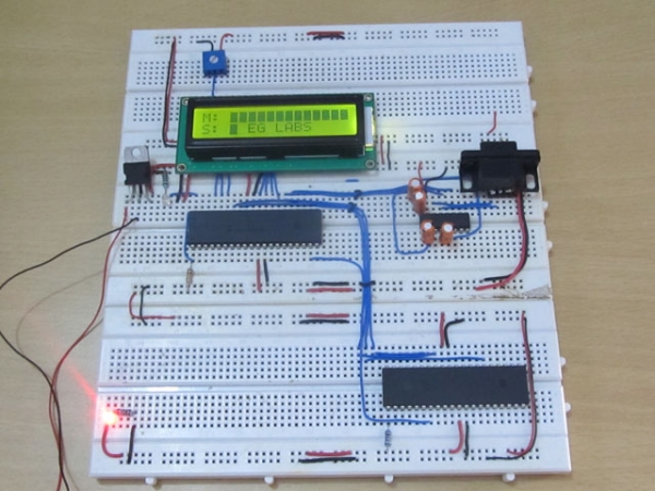
Parts used in the SPI Communication Project:
- PIC18F4550 Microcontroller
- Synchronous Serial Port Buffer (SSPBUF) Register
- Synchronous Serial Port Status (SSPSTAT) Register
- Synchronous Serial Port Control 1 (SSPCON1) Register
- SPI Bus Wires (SCK, MOSI, MISO)
- Master Device
- Slave Device
The Serial Peripheral Interface (SPI) is a high speed, synchronous, serial communication standard. This communication protocol is basically a Master Slave implementation where the master device controls the clock based on which the slave devices operates. The master can communicates with one or more slave in the system through SPI bus.
The SPI bus requires a minimum of three wires i.e. a SDO (Serial Data Out), SDI (Serial Data Input) and SCK (Serial Clock). Since it is a master controller system the SDO is also called MOSI (Master Output Slave Input) and the SDI is also called MISO (Master Input Slave Output).The SPI is a full-duplex high speed communication protocol. The master and slave can transmit and receive data at the same time. The master generates clock for all these data transmissions.
In PIC18F4550 microcontroller the hardware implementation for the SPI interface can be viewed as a simple SISO (Serial-In-Serial-Out) Shift register controlled by a Clock.
The above diagram is a single buffer implementation of the SPI hardware. The data is shifted into the buffer from the slave device through the SDI (MISO) and the data is shifted out of the buffer to the slave through the SDO (MOSI). The only difference in the hardware configuration of a master and slave device is the direction of the clock. For a master device the clock is always output and for a slave device the clock is always input. The Clock unit generates the clock required for the data transmission. In case of a master device, the clock is generated by the device and all other devices in the SPI bus send or receive data to the master based on this clock. When the microcontroller is configured as a slave it can only accept the clock from a master device.
 On each clock generated or received one bit in the SISO register is shifted from the SDI to SDO. After the eighth clock since the communication starts, one byte of data has been shifted out through the SDO and one byte of data has been shifted in through the SDI. Now the SISO has an entire byte received from the slave while transmitting a byte to the slave. In PIC18F4550 the Serial Communication module is not dedicated for the SPI only, but it can be configured for IIC communication also. The entire module is called Master Synchronous Serial Port (MSSP) module. There are a few registers available in the PIC18F4550 which helps to configure the MSSP as an SPI master or slave module. The major registers associated with the SPI communication in the PIC18F4550 are SSPBUF, SSPSTAT and SSPCON1 register.
SSPBUF
The Synchronous Serial Port Buffer (SSPBUF) register is the register which holds the SPI data which needed to be shifted out to the slave or which has been shifted in from the slave. In case of a slave device this register holds the SPI data which needed to be shifted out to the master or which has been shifted in from the master. The data can be read or write into the register for receiving and sending. In a master mode the clock signal will be generated and the data starts shifted out as soon as it is written into the SSPBUF. In a slave mode the data which has been written into the SSPBUF will shifted out only when the master generates clock.SSPSTATThe Synchronous Serial Port Status (SSPSTAT) register is the register which holds the status of the SPI module. The first two bits and the last bit of this register are only dedicated for the SPI communication.
SMP:
This bit decides whether the master should sample the data receiving from the slave at the beginning or at the middle of the clock. The following figure shows a master which is sampling the data from the slave SDI at the end of the clock SCK.
The following table shows the function of SMP bit when its value is 0 or 1.
| 1 | Input data sampled at end of data output time |
| 0 | Input data sampled at middle of data output time |
When the microcontroller is configuring as a SPI slave the SMP bit should be cleared.
CKE:
This bit is significant for both the master and slave device since it decide whether the data should be transmitted on the clock transition from active to idle state.
In the following figure assume the clock low is the idle state, and then the data is transmitted through the SDO when the clock makes a transition from the active to idle state.
The following table shows the function of CKE bit when its value is 0 or 1.
| 1 | Transmit occurs on transition from active to Idle clock state |
| 0 | Transmit occurs on transition from Idle to active clock state |
BF:
This bit will get automatically set once eight bits are received in the buffer which makes the buffer full. The bit can hence be used to decide when the data can be read out. Before reading or writing to the SSPBUF the status of this BF bit should be checked till it becomes 1.
Whenever the BF bit is found to be set it means the transmission is complete or reception is complete, since in the SISO buffer implementation of the SSPBUF transmission of a byte happen along with the reception of another byte.
The following table shows the function of CKE bit when its value is 0 or 1.
| 1 | Receive complete, SSPBUF is full |
| 0 | Receive not complete, SSPBUF is empty |
In this particular project both the master and the slave are configured with SMP=0(slave mode), CKE=0(transmission on Idle to active clock state), BF = 0 and all other bits 0. Hence the value that can be written into the SSPSTAT register is;
SSPSTAT = 0x00;
SSPCON1
The Synchronous Serial Port Control 1(SSPCON1) register is the register which is dedicated register for the control of SPI only. All the bits of these register are significant and should be carefully set them.
WCOL:
This bit can be used to detect whether write collision has occurred or not. The write collision occurs when the data to be transmitted is written into the SSPBUF while it still transmitting the previous data.
The following table shows the function of WCOL bit when its value is 0 or 1.
| 1 | The SSPBUF register is written while it is still transmitting the previous word |
| 0 | No collision occurred |
SSPOV:
This bit is significant only in the slave mode. It is used to detect whether a data overflow has occurred or not. The data overflow is said to happen when already eight bits are shifted into the SSPBUF from the master and then a ninth bit shifts in. As the ninth bit shifts in the first ever bit which has been shifted into the SSPBUF will be lost. In such a situation a read operation on the SSPBUF will give a junk data.
To avoid this data error while receiving from the master the SSPOV bit will get set once an overflow occurs. The overflow can be prevented by simply by reading out the SSPBUF once it completes receiving eight bits.
The following table shows the function of SSPOV bit when its value is 0 or 1.
| 1 | Overflow occurred |
| 0 | No overflow occurred |
SSPEN:
This is the most important bit which enables the MSSP module as an SPI module. This bit is set for the first time when the SPI configuration is done. Resetting this bit during running of a program will reset the entire SPI module. When this bit is enabled the SCK, SDO, SDI and SS are configured as the SPI pins.
The following table shows the function of SSPEN bit when its value is 0 or 1.
| 1 | Enables serial port and configures SCK, SDO, SDI and SS as serial port pins |
| 0 | Disables serial port and configures these pins as I/O port pins |
CKP:
This bit decides whether the idle state of the clock should be the low level or the high level of the clock. This bit decides the polarity of the idle state while the CKE pin decides whether to send a data when the clock makes a transition from active to idle state or idle to active state.
The following table shows the function of CKP bit when its value is 0 or 1.
| Idle state for clock is a high level | |
| 0 | Idle state for clock is a low level |
SSPM3 SSPM2 SSPM1 SSPM0:
This group of four bits decides whether the microcontroller should act as a master or slave. According to the bit combination this bits can enable or disable the SS control on the slave’s SPI module and to select the master’s SPI clock frequency.
The following table shows the meaning of different bit combinations for these four bits;
| 0101 | SPI Slave mode, clock = SCK pin, SS pin control disabled, SS can be used as I/O pin |
| 0100 | SPI Slave mode, clock = SCK pin, SS pin control enabled |
| 0011 | SPI Master mode, clock = TMR2 output/2 |
| 0010 | SPI Master mode, clock = FOSC/64 |
| 0001 | SPI Master mode, clock = FOSC/16 |
| 0000 | SPI Master mode, clock = FOSC/4 |
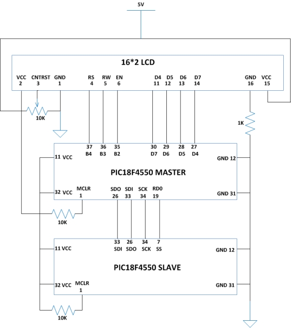 In this project the master microcontroller is initialized with SSPEN = 1 (enable serial port), SSPM[3-0] = 0b0010 (master mode, clock =FOSC/64), all other bits are zero. Hence the value that should be written into the SSPCON1 register is;
SSPCON1 = 0x22
The slave microcontroller is initialized with SSPEN=1(Enable SPI), SSPM [3-0] =0100(SPI Slave mode, clock=SCKpin,SSpin control enabled). Hence the value that should be written into the SSPCON1 register is;
READ AND WRITE OPERATIONS
The SSPBUF register can be read or write just like any other normal register, but care should be taken not to overwrite the data which is still in transmission and should read the data before the buffer overflows. Both the write overflow and the buffer overflow can be avoided by checking the BF bit in the SSPSTAT register before reading and writing into the SSPBUF. The program should wait till the BF flag becomes 1 before reading from the buffer or writing into the buffer.
There is a slight difference in the way in which the master and slave device should perform read and write. For a master it simply writes the data into the SSPBUF to initiate a transmission. Then it should wait for the BF flag to become high before it could read the data and the writing of the next byte follows the read operation. Slave on the other hand waits for the BF flag to become high and then it reads the data and writes the data.
For more detail: How to use PIC18F4550 as a SPI Slave Transmitter
- How many wires does the SPI bus require?
The SPI bus requires a minimum of three wires: SDO (MOSI), SDI (MISO), and SCK. - What is the function of the SMP bit in the SSPSTAT register?
The SMP bit decides whether the master samples input data at the beginning or middle of the clock cycle. - When does the BF bit get set automatically?
The BF bit gets set once eight bits are received in the buffer, indicating the buffer is full. - What happens if the SSPOV bit is set during operation?
An overflow has occurred where a ninth bit shifted in after eight were already received, potentially causing junk data. - Which bit enables the MSSP module as an SPI module?
The SSPEN bit enables the serial port and configures the relevant pins as serial port pins. - How do you configure the PIC18F4550 as a SPI Master with FOSC/64 clock?
Set SSPEN to 1 and SSPM[3-0] to 0b0010 in the SSPCON1 register. - What is the correct initialization value for the SSPSTAT register in this project?
The value written into the SSPSTAT register is 0x00 based on the specified configurations. - How should a slave device handle read and write operations?
The slave waits for the BF flag to become high before reading data and then writes new data.