Ensuring a perfect PCBA development requires meticulous planning, designing and manufacturing processes. To ensure avoidance of any mistakes or errors in PCBA manufacturing, it is essential to know some common issues that can cause error in the overall assembly. This article revolves around some common issues encountered during PCB assembly design along with recommendations to avoid them so that you can rectify such errors at the earliest stages.
What is PCBA?
PCBA stands for Printed Circuit Board Assembly. It involve the integration of a PCB with electronic components and accessories. In short, PCBA is the PCB equipped with assembled electronics components as shown in the figure below.
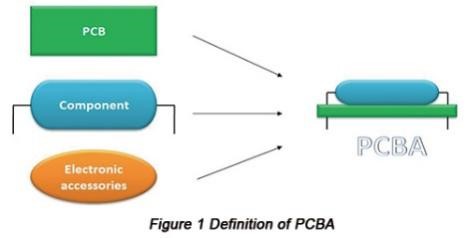
Printed Circuit Boards (PCBs), are meant to bear integrated circuits (ICs) and components. When completely developed, we call them PCBAs upon full assembly. PCBAs have become smaller and more intricate as compared to the past, given the escalating demand for cutting-edge technology.
The electronics manufacturing industry begins with the design phase, just like any other product development field. Printed Circuit Board Assembly (PCBA) design process involves developing the schematics, layouts and design files for Printed Circuit Boards (PCBs), which will eventually include the assembled components onto it. The impact of PCBA design on manufacturing of the final product is vital. Therefore, getting PCBA design right is paramount, which demands meticulous attention.
Common Types of Errors in PCBAs
In the fast developing electronics industry, engineers and designer must equip themselves with fundamental issues. Following are four types of design errors in PCBAs:
Component Placement Issues
This category includes errors like component misalignment, insufficient spacing, and improper orientation. They can lead to functionality and reliability issues.
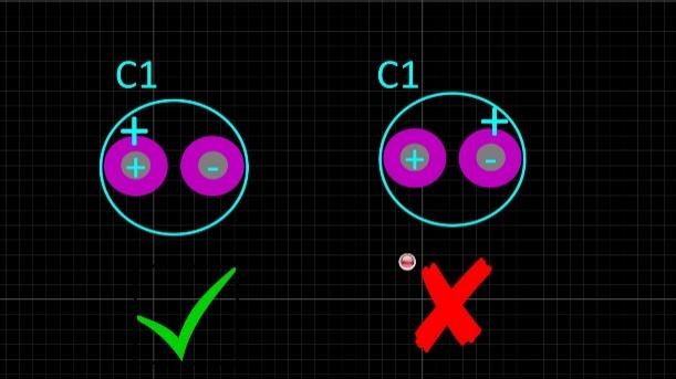
One of an important issue is incorrect orientation. Placing components in the incorrect orientation will lead to revered polarity and improper functionality of the circuit board. To avoid such an issue, review the datasheet of polarized components like diodes, capacitor etc, carefully. In the next figure you see the wrong marking of Pin 1 of electrolytic capacitor.
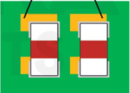
Similarly, misaligned components can cause soldering issues and tombstoning. Tombstoning is an effect where one end of the component lifts from a pad of the PCB during reflow soldering process and affects mainly surface mount components. Therefore, in PCBA designing, proper placement of pins and connectors is essential for smooth signal transmission. Incorrect placement may damage connectors. This results in using pattern-matching tools and telecentric lenses for rectification by the manufacturer. In the next figure, we see component misplacement.
The components are misplaced from the pads
In order to avoid these component placement issues, following measures can be taken:
- To include clear outlines for components on the design of a PCB and adding centroid for reference.
- To create a 1:1 ratio between solder mask opening and pads.
As illustrated in the previous figure, the component shift is a common defect during PCB assembly. It is caused by various factors like, reflow tension and poor solder placement. The effective strategies to avoid component shift during the manufacturing process are maintaining optimal humidity and temperature levels, minimizing movement, and application of flux are effective strategies to prevent component shift. Adhering to design rules and stencil modifications further mitigate the risk of missing parts.
Routing Issues
Routing is one of the most important factor in PCBA design. Un-routed signals and shorted circuits pose significant challenges in PCBA design. The next figure shows an un-routed net in the PCB design.
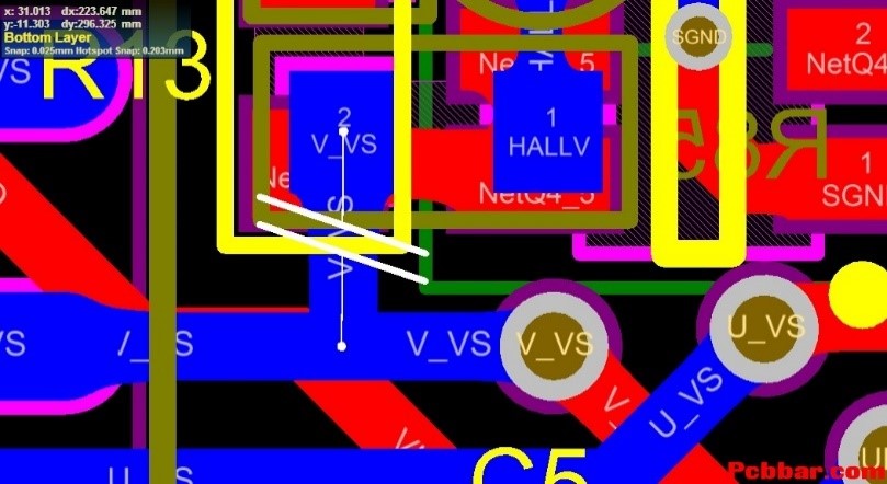
Incomplete connections between components result in open circuits, potentially causing malfunctions and overheating. Crosstalk, impedance mismatches, and signal integrity issues may also arise due to routing errors. Incomplete connections or wire breaks are a frequent issue during PCB manufacturing and assembly. Following image shows an incomplete connection that may seem fine in a zoomed out version of the layout.

In order to prevent such an issue, one must have proficiency in designing PCB layouts for PCBA. Most of the PCB designing tools like Altium designer allows the user to detect these incomplete or un-routed tracks automatically in designing process. The Design Rule Checking system in Altium and Proteus, provides an overview of the unconnected routes and identify them with symbols and lines. But during the manufacturing and assembly process, detecting wire breaks can be challenging and lead to boards functioning intermittently or failing prematurely. To rectify these wire beaks, thorough inspection is crucial to ensure cost and time saving. The PCBAs from reputable manufacturers are subjected to rigorous inspection procedures to mitigate instances of wire breaks.
Components Spacing and Clearance Issues
Keeping the component clearance to optimize the space without hurting the functionality is an important issue in PCB assembly. In order to avoid assembly errors originating from insufficient component clearance, following guidelines are recommended:
- A clearance of 6mil should be kept between components smaller than 0603 packages.
- Components like connectors, electrolytic capacitors, crystals etc, need a minimum spacing of 20 mil.
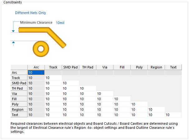
- At least 10 mil clearance must be kept between components of all size. The following image shows a Pad to trace clearance of 10mil.
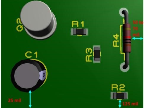
Moreover, the components placed on the board edge can be more susceptible to damage during handling. That is why, they might not be properly soldered during reflow soldering. To provide adequate clearance for cutting tool, you can position the components to 50-70 mil away from the board edge. But for taller components, make this board to component spacing at least 125 mil. Similarly, for the spacing between SMD components and board edges is recommended to be 20-25mil. Following is an illustration of these guidelines.
Heat Management Issues
With increasing component density, thermal management has become critical task. Overheating can damage PCBs and compromise circuit integrity. The insufficient heat management increases the operating temperature of the components. This can be avoided by strategic component placement and thermal analysis and using proper cooling mechanism. The cooling mechanism include using heatsinks, thermal vias and fans to dissipate the excessive heat and allow seamless functioning. However, identifying the hotspots and optimizing the components placement in that area can also significantly increases the heat dissipation. Following are the images of heat sinks, thermal vias and fans on different PCBs respectively.
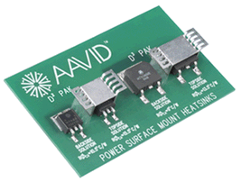
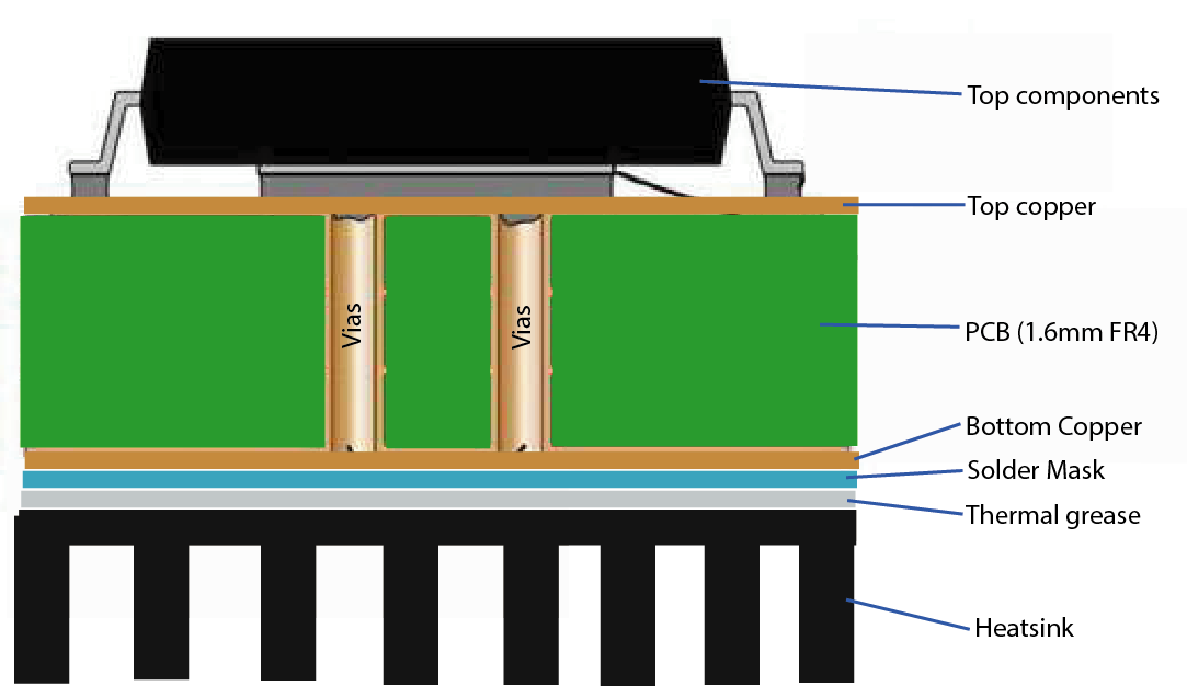
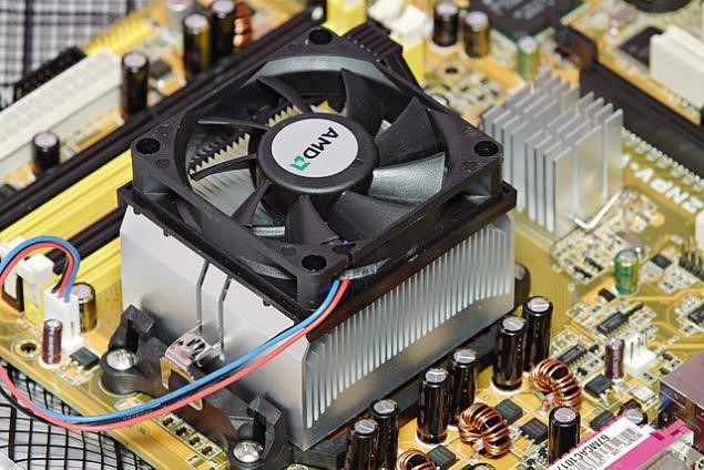
Therefore, effective heat dissipation is crucial for preventing component overheating. As shown in the above images, proper usage of heat, vias and fans according to the application is an essential measures to avoid component malfunctioning. To enhance the PCBA reliability, usage of the correct size and shape of SMD heat sinks ensures optimal heat dissipation. Also, to avoid these errors, one must adhere to best practices and leverage advanced design tools and simulation software. Addressing PCBA design errors early in the process is essential for delivering reliable electronics at scale.
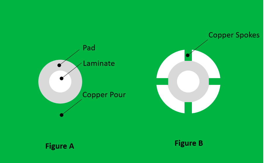
In case of through-hole components, the insufficient thermal relief can obscure the heat dissipation required for the right operation of that component. This may lead to poor reliability of solder joint of the component. Therefore, the footprint of such components should be designed to ensure proper heat transfer during soldering. Use minimum of 4 spokes evenly distributed around the pad for sufficient heat dissipation. A thermal relief pad is a technique used in PCB design to reduce thermal stress problems. It includes copper spokes that extend from the pad to the surrounding copper plane. The spoke width should be 1/3 of the pad’s diameter as shown in the following figure.
Conclusion
In conclusion, the designing, manufacturing and assembly processes of PCB are very intricate and require attention to detail. From components placement to thermal management, each step presents its own challenges and issue. And these issues are not limited to designing errors only, but there are some errors that occur during the manufacturing and fabrication processes as well. Therefore, a clear understanding of common manufacturing defects is vital to avoid producing low-quality boards. This article discusses some common types of issues in PCBAs and their solutions for engineers or designers to facilitate a smooth PCBA designing and manufacturing process. Moreover, some manufacturing issues were also discussed that are resolved with high-end inspection equipment available with the reliable manufacturers for developing quality PCB assemblies.
