Summary of 650V, 100A GaN transistors on show
GaN Systems will unveil the GS66540C, a 650V 100A gallium nitride power transistor, at EPE'15. Based on proprietary Island Technology and GaNPX packaging, this device eliminates wirebonds to achieve ultra-low thermal losses and fast switching rates exceeding 100V/nsec. Designed for solar, industrial, and automotive markets, it offers significant performance improvements over traditional silicon MOSFETs and IGBTs.
Parts used in the GS66540C Project:
- GS66540C 650V 100A high current GaN power transistors
- GaNPX packaging
- Island Technology die design
- Drive Assist technology
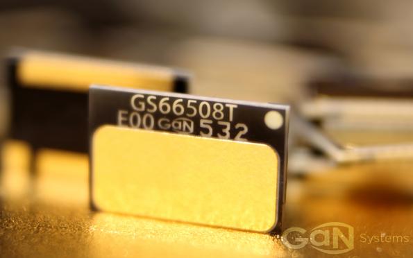
The GS66540C (the picture is of a prior, lower-current part) high current power devices will be revealed for the first time. Part of the company’s family of 650V gallium nitride power transistors based on its proprietary Island Technology, these high density devices achieve extremely efficient power conversion with fast switching rates of >100V/nsec and ultra-low thermal losses. The GS66540C is supplied in an evolved form of GaNPX packaging specially developed for higher operating currents, providing lower inductance and greater surface mount mechanical robustness required by power modules for the industrial and automotive markets.
The near-chipscale parts have no wirebonds and offer step-change improvements in switching and conduction performance over traditional silicon MOSFETs and IGBTs. Parts are, the company says, being designed in to solar, industrial and automotive applications as global manufacturers race to use the power of GaN to secure competitive advantage.
GaN Systems positions itself as the first company to have developed and productised a comprehensive portfolio of GaN E-HEMT power devices with current ratings from 7A to 250A, in both 650V and 100V ranges. GaN Systems’ Island Technology die design, combined with the extremely low inductance and thermal efficiency of GaNPX packaging and Drive Assist technology, provides its GaN E-HEMTs with a claimed 45x improvement in switching and conduction performance over silicon MOSFETs and IGBTs.
For more detail: 650V, 100A GaN transistors on show
- Where will the GS66540C be displayed for the first time?
It will be revealed at the 17th Conference on Power Electronics and Applications, EPE'15 - ECCE Europe at CERN in Geneva. - What technology does the GS66540C use for its die design?
The device uses the company's proprietary Island Technology. - How fast are the switching rates of these high density devices?
They achieve extremely efficient power conversion with fast switching rates greater than 100V per nanosecond. - Does the GS66540C contain wirebonds?
No, the near-chipscale parts have no wirebonds. - Which markets require the mechanical robustness provided by the evolved GaNPX packaging?
The packaging provides the robustness required by power modules for the industrial and automotive markets. - What is the claimed improvement in performance over silicon MOSFETs and IGBTs?
The combination of technologies provides a claimed 45x improvement in switching and conduction performance. - What current ratings are available in the comprehensive portfolio of GaN E-HEMT power devices?
The portfolio includes current ratings from 7A to 250A. - In what voltage ranges does GaN Systems offer its E-HEMT power devices?
The devices are available in both 650V and 100V ranges.