Summary of TFT-LCD Production Process Explained
Summary: LG Display explains the TFT-LCD manufacturing steps, focusing on the TFT process that builds microscopic transistors on a glass substrate. The process includes substrate cleaning, film deposition, and photo-resist coating to form layered structures that become pixels and control liquid crystal movement.
Parts used in the TFT-LCD Production Process:
- Glass substrate
- Film layer (deposited material)
- Photo-resist (light-sensitive coating)
- Transistor structures (micro switches)
- Liquid crystal layer (controlled by transistors)
- Pixels (rectangular pixel sections)
Ever wondered how the TV and monitor displays you use every day work? The TFT-LCD manufacturing process consists of a set of processes for producing TFT, color filtering, cell, module and others. LG Display Newsroom gives a detailed, but easy to follow explanation of the entire steps below.
Close Look at the Thin Film Translator (TFT) Process
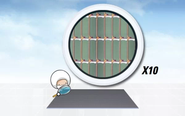
Let’s take a closer look at the production process for a TFT board, the bottom-most layer of an LCD panel. The image above depicts a TFT board, which consists of rows of small rectangular sections that together resembles a chessboard. Each rectangular section is a pixel, and each pixel contains a transistor that controls its function. The TFT process is the process that builds these transistors on top of a glass substrate.
So, what exactly is a transistor? Simply described, a transistor is a microscopic switch that controls the flow of electricity in the direction of liquid crystal and regulates the movement of the liquid crystal.
On top of a TFT board are millions of tiny transistors that are invisible to the naked eye, each of which are one hundredth of the thickness of a single strand of hair. If you examine the transistor up close, you would notice that it consists of several layers. Now, let’s see how each layer is produced, starting with the first layer.
After cleaning the glass substrate (Cleaning), it is coated with a layer of film, which is essential in creating the appropriate shape (Deposition). Then, a layer of light-sensitive material is spread out on top of this film (Photo-resist coating). Through these steps, we can create two layers, on which we can build parts of a transistor of various shapes and sizes as you can see in the picture above.
For more detail: TFT-LCD Production Process Explained
- What is the TFT process?
The TFT process builds transistors on a glass substrate that act as microscopic switches for each pixel. - What is a transistor in a TFT-LCD?
A transistor is a microscopic switch that controls the flow of electricity and regulates liquid crystal movement. - Where are transistors formed?
Transistors are formed on the TFT board, the bottom-most layer of an LCD panel, on top of a glass substrate. - How many transistors are on a TFT board?
Millions of tiny transistors are on a TFT board, one per pixel, and are invisible to the naked eye. - What are the initial steps in creating transistor layers?
Initial steps include cleaning the glass substrate, depositing a film layer, and coating with photo-resist. - Why is film deposition necessary?
Film deposition creates a layer essential for forming the appropriate shapes of transistor components. - What role does photo-resist play?
Photo-resist is a light-sensitive coating spread on the film to enable patterning of transistor layers.