Summary of Digital logic probe for troubleshooting TTL and CMOS circuits
This article details the construction of a universal digital logic probe capable of debugging both TTL and CMOS circuits. Unlike standard multimeters, this device automatically identifies logic states (High, Low, or Intermediate) without manual voltage calculations. The project utilizes a PIC12F683 microcontroller to measure supply voltage and determine appropriate logic thresholds dynamically. It features a seven-segment display driven by a CD4094 shift register, ensuring clear visual feedback for engineers troubleshooting complex digital systems with minimal components.
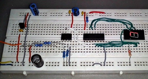
Parts used in the Universal Digital Logic Probe:
- 78L05 voltage regulator
- Microchip PIC12F683 microcontroller
- CD4094BE CMOS shift register
- Tiny seven segment display
- 9.1K Ohm resistors (1% tolerance)
- 1K Ohm resistors (1% tolerance)
A logic probe is considered as a stethoscope for engineers and technicians for debugging digital logic circuits that consists of logic gates, memories, registers, etc. A digital multimeter (DVM) can also be used for such analytical purposes but it gives you the numeric value of the voltage at a point instead of the logic state. Depending on whether the circuit is based on TTL or CMOS components, the voltage levels for logic 0 and 1 could be different for each family. DVM users, thus, have to calculate logic levels from the measured voltages, which consumes time and delays the troubleshooting procedure. A logic probe, on the other hand, does all these functions automatically and shows meaningful logic states at test points. In this project, we will discuss about making a digital logic probe that is applicable to both TTL and CMOS circuits and uses minimal components.
Theory
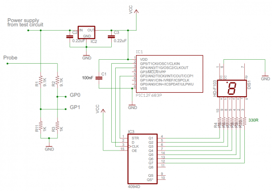
There are mainly two logic families used in digital circuits: TTL and CMOS. While TTL operates at +5V, the power supply for CMOS circuits could range from +3V to 15V. According to the standard TTL convention, any voltage less than 0.8V is defined as logic low while any voltage above 2.2 is defined as logic high and anything in between these extremes is defined as intermediate state. In case of CMOS circuits, any voltage less than 1/3 of VDD is defined as logic low while any voltage above 2/3 of VDD is defined as logic high. Any voltage between these values is defined as intermediate or transitional state. This logic probe works for both TTL and CMOS circuits powered from +5V to 15V.
This logic probe consists of a 78L05 voltage regulator, a Microchip PIC12F683 microcontroller, a CD4094BE CMOS shift register and a tiny seven segment display. Since the operating voltage range of this logic probe is between 5 to 15V, the role of the 78L05 voltage regulator is to ensure that the microcontroller and the rest of the circuit are always powered with a stable 5V source. There are two voltage divider networks, each made from a 9.1K and a 1K Ohms (1% tolerance) resistors. The outputs of the two networks go to the ADC channels AN0 and AN1. The AN0 channel reads the logic level voltage of the test pin whereas the AN1 channel is used to measure the supply voltage of the test circuit. The information of the supply voltage is necessary to identify a CMOS circuit powered with > 5V. The GP2, GP4, and GP5 pins of PIC12F683 drives the CD4094 shift register. The shift register acts as an I/O expander in this application and its outputs are connected to a seven segment display.
Software
The software for this project is written in MikroC PRO for PIC version 5.30. Only the ADC built-in library is used. The rest of the code is written without any library aid. The code starts with the definitions of pin names and common variable declarations. Apart from the main function which does all the tasks, there are six functions in the code. The setup() function sets directions of I/O pins and initiates the built-in ADC for data acquisition. The test_display() function tests the LEDs of the seven segment display connected to the shift register. The way this is done with the shift register will be discussed later in this text. The feature that makes this logic probe universal and unique is its ability to determine the supply voltage level. In the function test_supply(), the power source is tested. During this test if it is found that the ADC average of supply voltage is within the span of 4.75V to 5.25V then the standard TTL minimum high and maximum low logic level voltages are set, otherwise conventional CMOS logic level voltage values are set. These values are kept in the variables called high_level and low_level and are retained till power down. The display(unsigned char val) function is a software-hardware link between the shift register and the micro. It converts any 8 bit value given to the variable val in a way that it can be sent as an output just like a regular I/O port. The strobe pin is at first kept low to allow the access of the internal latches of the CD4094. Eight clock pulses are needed to shift data into the latches. During each clock pulse to the shift register, the variable val’s most significant bit (MSB) is read first and is sent as a data to the data input of the shift register. After sending data to the data pin, val is left shifted once and the clock pin is also toggled once. At the end of eight cycles the strobe pin is pulled high and the display is updated. The adc_avg(unsigned char ch) function read the designated ADC channel by taking 16 samples of ADC data and converting these samples into an average voltage value. Lastly the check_logic() function checks the logic input and sends logic symbol data to the seven segment display.
For more detail: Digital logic probe for troubleshooting TTL and CMOS circuits
- How does a logic probe differ from a digital multimeter?
A logic probe automatically shows meaningful logic states at test points, whereas a DVM provides numeric voltage values that require manual calculation to determine logic levels. - What is the operating voltage range of this logic probe?
The logic probe works for both TTL and CMOS circuits powered from +5V to 15V. - Why are two voltage divider networks used in the circuit?
One network connects to AN0 to read the logic level voltage of the test pin, while the other connects to AN1 to measure the supply voltage of the test circuit. - How does the software determine if a circuit is TTL or CMOS?
The code checks if the ADC average of supply voltage is within 4.75V to 5.25V; if so, it uses TTL logic levels, otherwise it sets conventional CMOS logic level values. - What role does the 78L05 voltage regulator play?
The 78L05 ensures that the microcontroller and the rest of the circuit are always powered with a stable 5V source regardless of the input voltage between 5 to 15V. - How many samples are taken for the ADC average calculation?
The adc_avg function reads the designated ADC channel by taking 16 samples of ADC data and converting these into an average voltage value. - Which pins of the PIC12F683 drive the CD4094 shift register?
The GP2, GP4, and GP5 pins of the PIC12F683 drive the CD4094 shift register. - How is data sent to the seven segment display via the shift register?
Eight clock pulses are needed to shift data into the latches, reading the most significant bit first, followed by toggling the clock pin, and finally pulling the strobe pin high to update the display.