Summary of Design your own Compact 5V/3.3V SMPS Circuit for Embedded and IoT Projects
This article details the design and construction of a compact, open-frame Switch Mode Power Supply (SMPS) delivering 5V or 3.3V at 1.5A for IoT devices like NodeMCU and ESP32. Utilizing the TNY284DG IC, the circuit accepts 85-230V AC input without an EMI filter to minimize size and cost. It features short-circuit protection, overvoltage protection, and hardware-configurable output voltage via a jumper. The project includes a specific BOM, schematic, and PCB layout instructions suitable for space-constrained embedded applications.
Parts used in the Compact 5V/3.3V SMPS:
- Fuse 1A 250VAC Slow Blow
- Diode Bridge DB107
- Capacitor 10uF / 400V
- P6KE Diode
- UF4007 Diode
- Resistor 2Meg Ohm (2 pcs)
- Capacitor 2.2nF 250VAC (2 pcs)
- TNY284DG IC
- Capacitor 10uF / 16V
- PC817 Optocoupler
- Resistor 1k Ohm
- Resistor 22 Ohm (2 pcs)
- Capacitor 100 nF
- TL431 Reference
- SR360 Schottky Diode
- Capacitor 470pF 100V
- Capacitor 1000uF 16V
- Inductor 3.3uH Drum core
A crude way to power your DC circuits with AC mains is to use a step-down transformer for stepping down the 230V mains voltage and adding a couple of diodes as a bridge rectifier. But due to the huge space size and other drawbacks, it cannot be used for all purposes. Another most popular and professional way is to use Switch Mode Power Supply Circuits for converting your AC mains into a wide range of DC voltage as required, almost every consumer electronics from normal 12V adapter to a Laptop Charger has a SMPS circuit to provide the required DC output power.
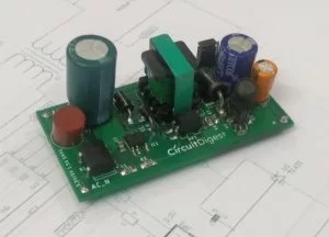
At circuitdigest, we have already built few popular SMPS circuits for different ratings, namely the 12V 1A Viper 22A SMPS, 5V 2A SMPS, and 12V 1A SMPS circuit each of which can be used for different applications. This time, we will build a SMPS that can be used for general purposes and has a simple module shape to be used in space-related situations. Nowadays, the Internet of Things uses various wifi-based processors like NodeMCU, ESP32, and ESP12E, etc. which operate on 5V or 3.3V. These modules are highly compact and hence to power these boards, it makes sense to use smaller SMPS circuits that can go on the same board, instead of using a separate SMPS circuit. Hence in this article, we will learn how to build a SMPS circuit that can either output 5V or 3.3V (hardware configurable using jumper), the circuit design and PCB layout is also provided, so you can simply port this into your existing design. Here our PCB boards are manufactured by PCBGoGo, a china based low cost high quality PCB prototype and PCB assembly service company.
The rating of the SMPS is 5V or 3.3V 1.5A as most of the development board uses 5V or 3.3V logic level voltages and 1.5A should be good enough for most of the IoT based applications. But do note that this SMPS does not have any filters in the input section to reduce size and cost. Therefore, this SMPS can be only used for powering microcontroller boards or charging purposes. Make sure that it will be covered from the user’s reach when in operation.
Warning: Working with SMPS circuits can be dangerous as it involves AC mains voltage which is potentially lethal. Do not attempt to build this if you have no experience working with AC mains. Always stay cautious with live wires and charged capacitors, use protective tools and supervision if required. You have been warned!!
5V/3.3V SMPS Board Specifications
The SMPS will have the following specifications.
- 85VAC to 230VAC input.
- 5V or 3.3V selectable 2A output.
- Open frame construction
- Short circuit and Overvoltage protection
- Small size with low-cost features.
Materials Required for SMPS Circuit (BOM)
- Fuse 1A 250VAC Slow Blow
- Diode Bridge DB107
- 10uF / 400V
- P6KE Diode
- UF4007
- 2Meg – 2 Pcs – 0805 package
- 2.2nF 250VAC
- TNY284DG
- 10uF / 16V – 0805 package
- PC817
- 1k – 0805 package
- 22R – 2pcs – 0805 package
- 100 nF – 0805 package
- TL431
- SR360
- 470pF 100V – 0805 package
- 1000uF 16V
- 3.3uH – Drum core
- 2.2nF 250VAC
Note: All parts were selected to be easily available for designers. The SMPS transformer has to be custom build using this datasheet. You can either use a vendor to built one or design and wind your SMPS transformer using the link.
This SMPS is designed using power integration IC TNY284DG. This SMPS Diver IC is best suitable for this SMPS as the IC is available in SMD package as well as the wattage is suitable for the purpose. The below image is showing the wattage specification of TNY284DG.
As we can see, TNY284DG is perfect for our option. As the construction is an open frame, it will match the output wattage of 8.5W. Meaning it can easily provide 1.5A at 5V.
5V/3.3V SMPS Circuit Diagram
Construction of this SMPS is pretty simple and straight forward. This design uses the Power Integration chipset as a SMPS driver IC. The schematic of the circuit can be seen in the below image-
Construction and Working
Before going straight into building the prototype part, let’s explore the circuitry operation. The circuit has the following sections-
- Input Protection
- AC-DC conversion
- Driver circuitry or Switching circuit
- Under-voltage lockout protection.
- Clamp circuit
- Magnetics and galvanic isolation
- EMI Filtering
- Secondary Rectifier and snubber circuit
- Filter Section
- Feedback section.
Input Protection
F1 is a slow blow fuse that will protect the SMPS from high load and fault conditions. The SMPS input section does not use any EMI filter considerations. This is a 1A 250VAC slow blow fuse and that will protect the SMPS in fault conditions. However, this fuse can be changed to a glass fuse. You can also check out the article on different types of fuse.
AC-DC Conversion
B1 is the diode bridge rectifier. This is DB107, a 1A 700V diode bridge. This will convert the AC input to the DC voltage. Additionally, the 10uF 400V capacitor will be essential for rectifying the DC ripple and it will provide a smooth DC output to the driver circuit as well as the Transformer.
Driver Circuitry or Switching Circuit
It is the main component of this SMPS. The transformer’s primary side is properly controlled by the switching circuit TNY284DG. The switching frequency is 120-132 kHz. Due to this high switching frequency, smaller transformers can be used.
Source: Design your own Compact 5V 3.3V SMPS Circuit for Embedded and IoT Projects
- What is the primary purpose of this SMPS circuit?
The circuit is designed to power IoT-based development boards like NodeMCU, ESP32, and ESP12E that require 5V or 3.3V. - Can the output voltage be changed on this board?
Yes, the output can be configured as either 5V or 3.3V using a hardware jumper. - Does this SMPS include an EMI filter in the input section?
No, the input section does not use any filters to reduce size and cost. - What are the safety warnings associated with building this project?
Working with SMPS circuits involves lethal AC mains voltage, so experience with live wires and protective tools is required. - What type of transformer is needed for this design?
A custom-built SMPS transformer must be constructed using the provided datasheet link. - Is the SMPS construction enclosed or open frame?
The construction is an open frame design intended for integration into existing designs. - What is the maximum output current rating of this SMPS?
The SMPS provides a selectable 5V or 3.3V output at up to 1.5A or 2A depending on the configuration. - Which IC is used as the driver for this SMPS?
The Power Integration IC TNY284DG is used as the SMPS driver chip.