Introduction
The Handy Lab Buddy is a tool every ECE should have. The four features of this tool include a talking voltmeter, logic probe, voltage averager, and frequency measurer. As a cheap and accurate device that outputs whatever being measured through speakers, it’s one of its kind and an essential tool for lab work.
Summary
Have you ever tried to debug a circuit and just wished your voltmeter would talk to you? Or have you ever been too lazy to turn on and calibrate the oscilloscope to measure the frequency? Well, this is the device for you. There are four operating modes of the Handy Lab Buddy. The first mode is a voltmeter that measures voltages up to 5V and says the voltage measured through speakers. The second mode is a logic probe that beeps once in a low tone if the output voltage is low and beeps twice in a higher tone if the output voltage is high. The third mode, a feature unique to this device, is a voltage averager that takes multiple samples in succession (perhaps a noisy voltage signal) and calculates the max, min, and mean voltage and speaks the values over a speaker. The fourth and final mode measures frequency with great accuracy from about 10 Hz to 100 kHz and speaks the value over a speaker. A device capable of all these functions and a “talking” ability at a very cheap cost is not available in the market today and is very useful to the ordinary engineer not wanting to invest in an oscilloscope. As very enthusiastic electrical engineers, we decided to build this device – simply for our own benefit, as it helps tremendously when debugging circuits.
We used quite a few features of the Atmel Mega644 MCU to implement this system, such as speech generation and output, multiple ADC conversions, the output of the pulse width modulator (PWM), and some others.
High Level Design
Rationale and Sources:
In all honesty, this was a secondary project idea for us, originally suggested by Bruce Land. Our original project idea, the Electronic Dartboard (discussed later), had tremendous problems with the hardware in the later weeks of the design cycle that forced us to abandon it. As our working efficiency and debugging experience increased dramatically in those frustrating few weeks, we managed to start and finish this new project within the final days of the semester.
Background Math:
The first big challenge for us was to get sound bites from AT&T and convert them for appropriate use for the MCU. Using the speech generation document by Bruce Land, we utilized his MATLAB programs to downsample from 16 kHz to 8 kHz and create header C files. The compression used in the MATLAB program was a differential pulse-code modulation (DPCM) with a 4:1 compression which sends 2:1 derivative samples.
To calculate the voltage generated, we had to use the built-in analog to digital converter in the MCU. Simple bit conversions were done, and we had to divide the 10-bit digital voltage output by 1024 over VREF (5V) to get a floating point value for the voltage. For the logic probe, the same thing was done, except an additional comparison was made to a threshold. The third feature, calculating the min, max, and average of samples of voltages, used pretty much the same principle as above except used additional variables to store the previous mean, min, max and sample number of samples. Frequency is measured using an elegant combination of software and hardware. Our frequency hardware first filters out the DC component of any input, then reapplies a DC bias, resulting in an AC waveform around the biasing point of our high frequency inverter. The output of this inverter is then stabilized. The final wave is thus a clean square wave, which is then used to trigger the external interrupt on the microcontroller. The software then responds to the interrupt, first synching the timers to the waveform, then measuring the the period of the waveform. Finally, the period is converted into frequency. Using this method, we can reliably measure frequencies from 10Hz to 100,000kHz.
There were two ISRs, one of them controlled the part of the speech played using a table, based on a timer, and the other, an external interrupt, controls triggers when to measure the time elapsed from the previous trigger, to measure frequency.
The user-interface of the Handy Lab Buddy is as demonstrated above. In the first two modes, after the analog voltage measurement is done, the signal needs to only go through an ADC before output to the LCD and to the speakers. For mode three, the voltage averager, the user presses the button on the probe when he/she is ready to take samples, then releases it to stop taking samples. The display shows the final output and it is automatically spoken. The fourth mode, frequency measurment, the user first has to change the banana plug connection to the frequency measurement pin (because of circuit isolation, described later in detail), then the signal passes through an inverter circuit to digitize the analog signal, which then triggers the external frequency ISR on the microcontroller (described later). After measurement in software, it is outputted onto the LCD and speakers. The four buttons that determine the modes are operated by a basic debounce state machine.
Hardware/Software Tradeoffs:
The biggest tradeoff during this design project was our decision to completely scrap our original idea and use this one. Our original idea was to create an Electronic Dartboard, where a player would draw concentric circles on a whiteboard, a infrared camera (removed form a WiiMote) would then be calibrated to the circles and display them on an LCD. Then, the user would “shoot” an IR dart (laser) at the whiteboard, which the WiiMote camera would have picked up and drawn the location on the LCD. However, the WiiMote IR camera was not reliable enough outside of it’s original controller. On top of that, we concluded the large LCD we were planning to use was fried after much testing. We worked on these getting these two hardware components to work by going to lab a lot of extra times overthree weeks to no avail. Thus, due to faulty hardware and being incredibly pressed for time, we decided to switch to this project, which our professor had initially suggested in class. In retrospect, we’re glad we made that decision, as we were able to come out with a complete, working product in a short span of time. The detailed schematics and code for the old project are described later.
One tradeoff we faced was during the design of our frequency measurer. We wondered how to calculate the frequency. One way of doing it was to use an Fast Fourier Transform algorithm as linked on the course website. However, we realized that the DFT/FFT would take up too much processing power and memory because of the look up tables. Besides, our frequency measurement only needs to measure the most prominent frequency, and the DFT/FFT would be doing unnecessary computation. Thus, we decided to take more of a hardware based approach, by digitizing the signal by passing it through an inverter, then using an interrupt to calculate the frequency.
Relationship to Standards:
There were no relevant IEEE, ISO, ANSI, or DIN standards related to this project.
Existing Patents, Copyrights, Trademarks:
There were no existing patents or trademarks associated with our project. We did utilize Bruce Land’s code for the implementation of the LCD and drivers, and his MATLAB code for converting .wav files from TextToSpeech to .h files.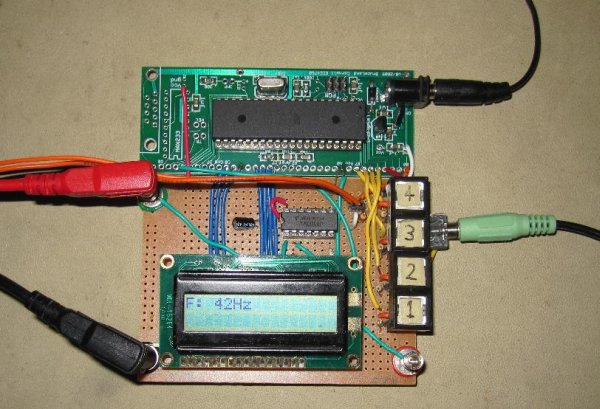
Project Design
Hardware Design:
The hardware design for the Handy Lab Buddy was rather simple. To program the Atmel ATMega644 Microcontroller, the STK500 development board was used. The Mega644 MCU was then put on the Custom PC Board, provided by the lab. Soldering components onto the PC Board had to be done with careful precision, as the pins were small and very compactly laid out.
Our other significant pieces of hardware in this project were the 2-line LCD display in lab, the 4 buttons, a speaker, an inverter, and probes (with another button). The overall interfacing of the MCU with the rest of the hardware is shown below in the schematic.
Buttons
Buttons 1-4 were connected to port B7 to B4 (respectively) of the MCU. The top pin was grounded, while each of the other pins had a 10kΩ connected to Vcc. The resistor was needed there because when a button is pressed, the wire is shorted – to prevent this a resistor was placed there. These buttons operated on a debounce state machine, described later in the Software Design section.
Another button was used as an interface for the voice output . This was also connected to a 10kΩ resistor to Vcc, and to port B0. When this button was pressed, depending on what mode the system was in, the system would speak whatever was on the LCD screen.
Frequency, Inverter, and Protector Circuit:
If a signal was to be measured for it’s frequency, it needed to go through a circuit first to be processed. First of all, the diode/resistor connected to Vcc in the schematic was just to protect the MCU port A0 from being fried in case a voltage greater than 5V is fed into port A0. The signal picked up by the probe goes through a 0.4uF total capcitance array to filter out DC values, then gets DC shifted by the voltage divider, before going through the inverter to shift the center voltage of the signal. The purpose of the inverter is to output a square wave from any periodic signal given. There were a few ways of accomplishing this, one using an inverter or another using a Schmitt Trigger op amp circuit. We chose the inverter because there was no analog circuitry to worry about. Thus, the “analog” wave gets converted to a digital wave, as it converts every point on the wave below the 2.5V threshold to a logic 0 and above the threshold to a logic 1. The output of this input is then stabilized by two 22 pF capacitors. The final wave going into port D3 is a clean square wave used to trigger the external interrupt of the microcontroller.
Speakers:
The speakers are not shown in the schematic. They were simply connected via a headphone jack from port B3 (output of the PWM) to ground.
Liquid Crystal Display:
The LCD used in this project was simply the 16-pin LCD used in ECE 4760 Spring 2010 Lab 1. The pin assignments are as in the schematic.
Microcontroller Operation:
The Atmel ATMega644 microcontroller was the control module of the device. Port A0 was the ADC used to implement the first three modes. Port D3 was used to implement the frequency mode. Port B0 was the button on the probe, that made the speaker output a voice signal, which was coming from port B3. Ports C0-C2 and C4-C7 were used for the LCD. The diagram shows how the microcontroller was laid out on the custom PCB board. The photograph after the probes section shows the completed target board connected to the rest of the circuit. Two 1 uF capacitors were also used to connect Vcc and Gnd to remove any external noise in the circuit as a whole.
For more detail: Cooper Bills (csb88) and Anish Borkar (ab673)