
Summary of DDS/PLL based VFO synthesizer using PIC16F876
This article describes a universal DDS/PLL VFO synthesizer designed for both transmitting and receiving, overcoming the spurious signal limitations of standard DDS chips like the AD9850. By integrating a PLL cleaning loop where the DDS acts as a programmable fractional divider, the design achieves precise tuning steps with low noise. The system is controlled by a PIC16F876 microcontroller and features a 6-digit LED display, rotary encoder, and push-buttons, all mounted on a single main board to support HF spectrum coverage for QRP applications.
Parts used in the DDS/PLL based VFO synthesizer:
- Analog Devices AD9850 or AD9851 single-chip DDS system
- 100MHz reference oscillator (for AD9850) or 180MHz clock input (for AD9851)
- 5th or 7th order low-pass LC filter
- Two 74HC74 R/S flip-flops for PLL detector
- VCO (Voltage Controlled Oscillator)
- PIC16F876 microcontroller
- 6 digit LED display
- Rotary incremental encoder (2 x 100 pulse 90 deg phase shifted outputs)
- Two push-buttons
- Main-board (86mm x 64mm)
- 21-pin header
DDS (Direct Digital Synthesized) VFO seems to be very popular among amateurs in last few years, mainly thanks to cheap and easy available single-chip DDS synthesizers. There are plenty of different amateur designs, some of them also available in a KIT form. They mostly use Analog Devices AD9850 or AD7008 single-chip DDS system to generate RF output directly. Such solution is acceptable and welcome as a VFO in small (QRP) transmitters. With only one IC it is possible to generate the CW output signal in a very wide range, for example with AD9850 and 100MHz reference oscillator it is easy to cover the complete HF spectrum (0 … 30MHz) in virtually infinite small steps (0,024Hz !!!). A simple low-pass LC filter of 5th or 7th order at the output easy handles the spurious signals to stay 60 to 70dB under the CW carrier.
Problems appear when one wants to use such VFO as a main mixing VFO at the 1st (front-end) mixer in a receiver. The unwanted spurs, which are suppressed relatively to the carrier (only) 60dB or 70dB, and there is plenty of such signals at the output of a DDS chip with 10 bit A/D, usually result in the reception of many out of band signals and produce high level of background noise at the RX output. Reception of let’s say 40m band in central Europe with such receiver is acceptable during the day but becomes hardly possible at the evenings due to quite a big number of broadcast transmitters, transmitting only few hundreds of kHz away from amateur band with the powers of 30 or 40dB stronger than typical (not QRP J) amateur TX, therefore impossible to filter them out by a reasonably complex preselection filter at the RX input.
When I’ve decided to build a DDS based VFO, the goal was to build a universal synthesizer usable for transmitting as well as for receiving purposes. To satisfy these requirements it was necessary to implement some cleaning of the signal at the output of the DDS chip. The natural choice was a PLL cleaning loop. I’ve chosen a rather unusual configuration of the DDS / PLL circuitry. There is a simple PLL detector built around two 74HC74 R/S flip-flops and the DDS is used as a programmable divider, dividing the VCO output signal in the PLL loop-back path in a fractional way. This makes it possible to achieve very small tuning steps without a big division ratio in a PLL loop-back divider. The maximum VCO frequency equals to the maximum allowed reference clock input frequency of the DDS chip and are 180MHz for AD9851.
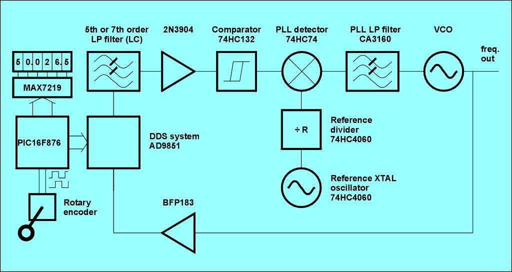
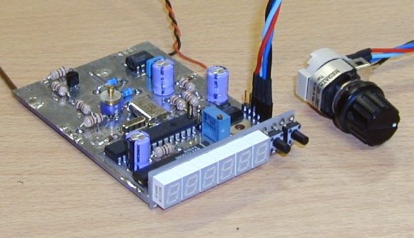
The use of more common AD9850 is also possible, only that the maximum VCO frequency drops to 125MHz. With a simple prescaler a higher VCO frequencies could be implemented. Both circuits, DDS / PLL loop as well as PIC16F876 controlling the DDS chip and user interface (6 digit LED display, rotary incremental encoder, two push-buttons) are implemented on a single 86mm x 64mm main-board. The 6 digit LED display and push-button board are attached directly to the main board through a 21-pin header. Rotary incremental encoder with 2 x 100 pulse 90 deg. phase shifted outputs allows the tuning rate of 400 steps per turn. Two tuning steps are selectable in the setup menu – slow and fast. Fast tuning is activated during the simultaneous turn of the tuning knob and activation of a key. A clarifier (R.I.T.) function is also available.
For more detail: DDS/PLL based VFO synthesizer using PIC16F876
- Why are standard DDS VFOs problematic for receiver front-ends?
Unwanted spurs suppressed only 60 to 70dB below the carrier cause reception of out-of-band signals and high background noise. - How does this project clean the signal from the DDS chip?
It implements a PLL cleaning loop where the DDS is used as a programmable fractional divider in the PLL loop-back path. - What is the maximum VCO frequency for the AD9851 configuration?
The maximum VCO frequency equals the maximum allowed reference clock input frequency of the DDS chip, which is 180MHz. - Can the AD9850 be used instead of the AD9851?
Yes, but the maximum VCO frequency drops to 125MHz unless a simple prescaler is added for higher frequencies. - Which microcontroller controls the DDS chip and user interface?
The PIC16F876 microcontroller handles the control of the DDS chip and the user interface components. - What tuning resolution does the rotary incremental encoder provide?
The encoder allows a tuning rate of 400 steps per turn with two selectable tuning speeds in the setup menu. - How is fast tuning activated on this device?
Fast tuning is activated during the simultaneous turn of the tuning knob and activation of a key. - Does the design include a clarifier function?
Yes, a clarifier (R.I.T.) function is available in the design.
