Summary of CLOCK MULTIPLIER – CRYSTAL FREQUENCY GENERATOR USING PT7C4511
This project is a low-cost, high-performance clock multiplier using PLL techniques to generate up to 200 MHz from a lower-frequency crystal or clock input. It supports crystal oscillator, clock multiplication, and frequency translation, offers nine selectable multiplication factors via jumpers, an output enable (tri-state) pin, low jitter, and adjustable crystal load capacitors for proper crystal loading.
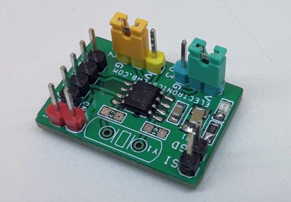
Parts used in the CLOCK MULTIPLIER – CRYSTAL FREQUENCY GENERATOR USING PT7C4511:
- PT7C4511 PLL clock multiplier IC
- Crystal Y1 (parallel resonant, fundamental mode, 5 MHz to 30 MHz)
- Capacitor C1 (crystal load/trimming)
- Capacitor C2 (crystal load/trimming)
- Additional crystal capacitors from X1 and X2 to ground (value = 2 x crystal load capacitance minus stray capacitance)
- Input connector CN1 for clock input
- On-board jumpers (J2, J3 and others) for selecting nine multiplication factors
- Output enable pin circuitry (for tri-state output control)
- Power supply connection (5 V DC, range 3 to 5 V DC)
- PCB (25.72 x 17.94 mm) with required traces and pads
This is an easy-to-build project and it is the most cost-effective and high-performance frequency multiplier, which instigates analog phase lock loop techniques. The circuit provides high-quality, high-frequency output from lower frequency crystal or clock input. The project can be used as a crystal frequency oscillator, clock multiplier and frequency translation. Using phase-locked-loop (PLL) techniques, the device uses a standard fundamental mode, inexpensive crystal to produce an output clock up to 200Mhz. On-board jumpers are provided to select from nine different multiplication factors, which output many common frequencies. The device also has an output enable pin that tri-states the clock output when the enable pin is taken low. The chip is intended for clock generation and frequency translation with low output jitter.
Refer to the table below for jumper settings to change the frequency multiplexing.
- Connections for Clock Input: CN1 Clock input 1- 50Mhz, Use J2, and J3 for frequency output settings.
- For Internal Clock Generator: Use crystal Y1, Capacitor C1, and C2
A parallel resonant, fundamental mode crystal should be used. The device crystal connections and capacitor connections are provided. These capacitors are used to adjust the stray capacitance of the board to match the nominally required crystal load capacitance. Because load capacitance can be only be increased in this trimming process. Crystal Capacitors, if needed, must be connected from each of the pins X1 and X2 to the ground.
The value (in pF) of these crystal capacitors should equal C-L x 2 in this equation, C-L=crystal capacitance in pF. Example: For a crystal with a 15pF load capacitance, each crystal capacitor would be 30pF.
FEATURES
- Power Supply 5V DC (Range 3 to 5 V DC)
- Zero ppm multiplication error
- Output Load 12mA Max
- Input crystal frequency of 5Mhz to 30Mhz
- Output Duty Cycle 50%
- Input Clock Frequency of 1-50Mhz
- Output Clock Frequencies up to 200Mhz
- 9 Selectable Frequencies Controlled by Jumper
- Peak to Peak Jitter Less than 200ps over 200ns Interval (100-200Mhz)
- Low Period Jitter 20ps (100-200Mhz)
- Tri-States Output for Board Level Testing
- PCB dimensions: 25.72 x 17.94 mm
Read more: CLOCK MULTIPLIER – CRYSTAL FREQUENCY GENERATOR USING PT7C4511
- What is the maximum output frequency of the device?
Output clock frequencies up to 200 MHz. - What input frequencies are supported for the crystal?
Input crystal frequency of 5 MHz to 30 MHz. - Can an external clock be used instead of the crystal?
Yes, CN1 accepts an input clock frequency of 1 to 50 MHz for external clock input. - How are different multiplication factors selected?
On-board jumpers are provided to select from nine different multiplication factors. - How is the crystal load capacitance adjusted?
Use crystal capacitors from each crystal pin to ground; each capacitor value should equal 2 times the crystal load capacitance (C-L x 2) to trim stray board capacitance. - What power supply voltage is required?
Power supply 5 V DC, with an operational range of 3 to 5 V DC. - Is there an enable or tri-state function on the output?
Yes, the device has an output enable pin that tri-states the clock output when taken low. - What is the specified jitter performance?
Peak-to-peak jitter less than 200 ps over 200 ns interval (100–200 MHz) and low period jitter of 20 ps (100–200 MHz). - What is the maximum output drive?
Output load 12 mA max. - What PCB size does the project use?
PCB dimensions are 25.72 x 17.94 mm.