Summary of Audio Spectrum Analyzer
Summary: We built a real-time audio spectrum analyzer using two Atmel Mega1284 MCUs: one for ADC sampling and FFT (FFT MCU) and one for visualization and composite NTSC video output (Video MCU). Audio (via 3.5mm jack) is amplified, low-pass filtered to 4 kHz, sampled at 8 kHz, transformed with a 128-point fixed-point FFT, and 32 frequency-bin magnitudes are sent via synchronous USART to the Video MCU, which renders a monochrome histogram on an NTSC TV. Users control range, scale, pause, and decay with push buttons.
Parts used in the Audio Spectrum Analyzer:
- Atmel Mega1284 microcontroller (two units)
- 3.5mm TRS female audio jack
- RCA female video jack (composite)
- LM358 operational amplifier
- Resistors (100kΩ, 39kΩ, 300kΩ, 100kΩ, 330Ω for buttons, and other resistors for DAC network)
- RC low-pass filter components (resistor and capacitor sized for ~3.7 kHz cutoff)
- Voltage divider for DC bias
- Crystal oscillator (16 MHz)
- Voltage regulators (on PC boards)
- Push buttons (4 total)
- DAC resistor network for video levels
- UART/USART wiring between MCUs including ready flag lines
- PCB boards / solder boards (audio board and main board)
- Male-to-male 3.5mm audio cable (user-supplied for input)
- Male-to-male RCA video cable (user-supplied for TV connection)
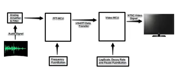
We developed an audio spectrum analyzer as our final project for ECE 4760. This analyzer presented a histogram-style representation of audio signals. We successfully achieved real-time display of the audio signal’s frequency spectrum using a monochromatic histogram layout, where bins extended from left to right, representing low to high frequency ranges. Our system was built around two Atmel Mega1284 microcontrollers.
These two microcontrollers had distinct roles: one managed audio data acquisition and processing (referred to as the FFT MCU), while the other handled visualization processing and video data transfer (referred to as the Video MCU). Users could choose from various display options by using a set of push buttons, including the overall frequency range displayed and the amplitude scale, among other settings.
To input an audio signal, users could connect any audio-producing device like a computer or an MP3 player to the device’s 3.5mm audio jack using a male-to-male 3.5mm audio cable. Furthermore, by employing a male-to-male RCA video cable, users could connect the device to any standard NTSC television with resolutions of at least 160×200 through the device’s RCA video jack, allowing them to visualize the audio data on the TV screen.
Our device was capable of displaying frequencies in audio signals up to 4 kHz, encompassing the typical frequency range of music, which was the primary input for our project, as illustrated in the accompanying diagram.
High Level Design
Rationale & Inspiration
Our project concept drew inspiration from popular toys like the T-Qualizer and the built-in music visualizers found in various software audio players such as Windows Media Player. Our goal was to create an affordable hardware-based equalizer that could seamlessly connect to standard audio inputs and video outputs. Initially, we considered using a microphone for audio input, but later realized that sourcing audio directly from another device provided a clearer signal.
The idea behind our project was twofold: firstly, to offer a captivating visual element that accompanies music, similar to the aforementioned entertainment sources, and secondly, to provide a means of visualizing the distinct frequency components associated with different sounds or instruments. For instance, this setup enables us to not only observe the fundamental pitch of an instrument, such as a saxophone but also to identify the various harmonics that contribute to the instrument’s timbre.
Overview
The data flow in our project follows a straightforward path. Initially, the audio signal is fed into the system through the audio jack. This signal undergoes amplification and filtering before being directed to the FFT MCU. Here, the audio signal is sampled at a consistent rate, and a Fast Fourier Transform (FFT) is applied to convert it into the frequency domain. The resulting frequency domain data is then forwarded to the Video MCU, which processes it in real-time, creating a histogram-style visualization. Users can customize the display by making adjustments through push buttons. Ultimately, the Video MCU sends a composite video signal to the TV.
Hardware and Software Tradeoffs
The primary trade-off concerning hardware and software revolved around the decision of whether to consolidate all computations on a single MCU, thus increasing software complexity, or to distribute the workload across two MCUs, introducing some additional hardware intricacies. This choice was necessitated by the requirement for precise audio sampling at specific intervals and the block-type nature of the FFT computation. Balancing these with the exact timing of video display and frame buffer creation while maintaining real-time processing proved challenging.
Ultimately, we opted to divide the tasks that demanded precise timing between two separate MCUs. Each MCU was assigned specific responsibilities, as elaborated in the subsequent software section. Although this approach entailed the extra hardware needed to connect the two MCUs and introduced some additional software intricacies for data transfer between them, these additional efforts were relatively minor compared to the complexities involved in attempting to execute all software operations on a single MCU.
Mathematical Background
To comprehend the process of sampling and transforming the audio signal into the frequency domain, it’s essential to grasp several fundamental signal processing concepts.
First and foremost, we must consider how the sampling rate is determined. We utilized an ADC channel on the FFT MCU to convert the analog audio input into discrete digital values. According to the Nyquist Sampling Theorem, the sampling rate should be at least twice the highest frequency present in the signal to prevent aliasing, which can distort the signal. We settled on a maximum input frequency of 4 kHz, as this covers most of the frequency range found in typical music without overwhelming the ADC. Consequently, we set the ADC sampling rate to 8 kHz.
Furthermore, we need to explore the conversion of the audio signal from its original time domain representation into a frequency domain representation. The Fourier transform is a mathematical algorithm that accomplishes this conversion. Different types of Fourier transforms are available, depending on whether the input is discrete or continuous, and whether the output should be discrete or continuous. Since we are dealing with finite digital systems, we opted for the Discrete Fourier Transform (DFT). The DFT transforms a discrete time audio signal, composed of a finite number of points N, into a discrete frequency signal with N points, commonly referred to as “frequency bins” in this context. Each point within the DFT represents a specific “bin” or frequency range. For purely real-valued signals like our audio signal, the frequency representation of the signal is symmetric around the (N/2)th point in the DFT. The highest bin encompasses frequencies up to the sampling frequency, while the lowest bin covers frequencies just above 0. Each bin shares the same frequency width, known as the frequency resolution, calculated as the sampling frequency divided by the number of bins N.
There are multiple algorithms that can calculate the DFT result more efficiently than directly applying the DFT equation. These algorithms, known as Fast Fourier Transform (FFT) methods, maintain the same precise result while reducing the computational complexity from O(N^2) of the DFT to O(N log2(N)). With larger values of N, this increase in speed significantly reduces computation time, particularly in software applications. Due to its recursive nature, it’s typically required that N be a power of 2. In our software, we implement a fixed-point number-based FFT algorithm, adapted from Bruce Land, to convert our discrete digital audio signal into discrete frequency bins.
Standards
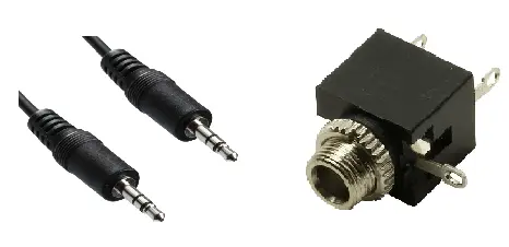
Our project incorporates various hardware and communication standards. In terms of hardware standards, we employed a conventional 3.5mm phone connector jack socket to accept analog audio signals into our device. Specifically, our device is designed to accommodate a three-contact TRS (tip-ring-sleeve) type male connector, which connects to our female jack. Although this three-contact design allows for the input of two-channel stereo audio, our device utilizes only one channel of the input, operating in mono audio mode.
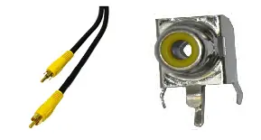
Furthermore, we utilized a standard RCA female video jack for the output, providing a composite analog video signal to a TV. This jack is designed for connection with a male RCA video plug. Both of these standard connectors are illustrated below.
In terms of communication protocols, we employed the NTSC analog television standard to deliver black and white video output to our NTSC-compatible television. NTSC, which stands for the National Television System Committee, serves as the prevalent analog video standard in most of North America. This standard specifies crucial parameters, such as 525 scan lines, two interlaced fields consisting of 262.5 lines each, and a scan line time of 63.55 microseconds. These NTSC standards were meticulously considered throughout our project to generate the composite video signal for our TV output.
Additionally, although not strictly classified as a standard, we utilized USART (Universal Synchronous Asynchronous Receiver Transmitter) for serial data transmission between our two MCUs. The Atmel Mega1284 MCU offers various frame formats that must be adhered to in both the transmitting and receiving MCUs, including the synchronous mode, which we implemented. While USART is frequently employed with communication standards like RS-232, it was not utilized in our project.
Hardware
Introduction
The hardware component of our project encompasses the two MCUs connected via USART, a hardware amplifier and filter circuit designed for audio input, user-operated push buttons for input control, and a DAC circuit for video output.
Audio Amplifier and Filter
First and foremost, our initial task involved calculating the input bias voltage offset for the analog audio signal to meet our specific requirements. This calculation considered two key factors: the amplifier’s range and the ADC reference voltage. The ADC reference voltage corresponds to the maximum value of the ADC (255), and any voltage exceeding this value would result in the maximum reading. We knew that the amplifier had a range from 0 to 3.5V, and the available ADC reference voltages were 1.1V, 2.56V, and 5V. After careful consideration, we selected the 2.56V reference voltage because the 5V option provided only about half the resolution, and values representing voltages above 3.5V were unnecessary. Using the 1.1V reference voltage wouldn’t fully utilize the op-amp’s range. Therefore, we decided to set the DC bias voltage at 1.28V to maximize the ADC range and ensure that the input signal remained within the op-amp’s range, preventing negative voltages. To achieve this, we designed a voltage divider using 100kΩ and 39kΩ resistors instead of the intended 34kΩ resistor, which elevated our DC bias voltage to 1.4V.
The Texas Instruments LM358 op-amp served as our primary amplifier component. By employing a non-inverting amplifier circuit, we established a gain of 4 (1 + 300kΩ/100kΩ). Initially, when we used a microphone as the input source, the gain was set to around 10 to amplify the weaker audio signal. This was because when an external audio source was used, the microphone required its own power source, resulting in a much stronger signal than the external source. However, when we switched to exclusively using audio directly from an external source, we reduced the gain since these audio signals were larger and easily adjustable. At a gain of around 10, we frequently reached the op-amp’s rail voltages. To reduce aliasing, we introduced an RC low-pass filter designed to eliminate frequencies above 4kHz. The RC time constant corresponded to a cutoff frequency of approximately 3.7kHz, although it featured a slow roll-off, and the RC filter transfer function did not drop below 0.5 until much higher cutoff frequencies. Therefore, we aimed to set the cutoff just slightly below our desired value of 4 kHz.
In the video below, you can observe a demonstration of how the analog audio signal appears after passing through this stage on an oscilloscope.
Push Buttons
Every push button featured a straightforward design. One of its ends was linked to the ground, while the other was connected to an input pin via a 330Ω resistor. The inclusion of the resistor served the purpose of safeguarding the ports against potential harm resulting from substantial current surges. Additionally, the MCU input had its pull-up resistor activated, rendering the port (and button) active low.
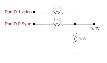
Video Digital-to-Analog Converter
To merge the digital video data signal (Port D.1) and the sync signal (Port D.0) into a composite analog video signal capable of producing three levels – 0V for sync, 0.3V for black, and 1V for white – we employed a straightforward DAC. This integration was facilitated by the resistor network situated to the right.
The resulting video output was linked to the inner axial pin of a standard female video RCA connector, while the outer ring of the RCA connector was connected to the common ground shared by the entire device.
Data Transmission Connections
We employed USART in synchronous mode for the purpose of transmitting data between the MCUs. This approach entailed the allocation of a dedicated port for the clock and another port exclusively for data transmission from the FFT MCU to the Video MCU. As data transfer from the Video MCU to the FFT MCU was not required, a third channel was not implemented. In addition to these channels, we also established three additional ports to facilitate the exchange of various flags and readiness signals between the two MCUs.
Color Generation
Initially, our objective was to enable our project to display color television. The plan involved the utilization of the ELM304 for sync pulse generation, the AD724 for converting RGB to a composite NTSC signal, and the video MCU for outputting RGB values. The sync output from the ELM304 was connected to both the HSync pin of the AD724 and two interrupt pins on the MCU. These interrupt pins served to determine the timing for outputting RGB values based on the occurrences of horizontal and vertical sync signals. These RGB values were subsequently connected to the inputs of the AD724, where they were transformed into a composite signal, which, in turn, was linked to the television. We assembled the circuitry, incorporating components such as the ELM304 and AD724, on a solder board. However, this setup was ultimately unused due to software-related challenges, as explained in the software section. You can review the schematic for this setup here.
Hardware Implementation
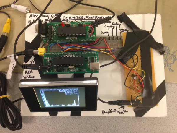
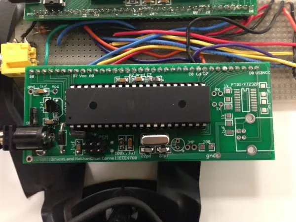
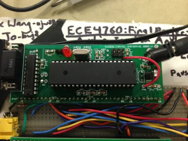
The Video MCU PC board, originally sourced from lab scrap, required some adjustments to ensure proper functionality. Specifically, we had to incorporate a new voltage regulator onto the board. In contrast, the FFT MCU PC board was meticulously constructed from a custom-designed PCB by Bruce Land and assembled according to the specifications provided on the associated documentation.
Both boards were equipped with the Atmel Mega1284 MCU. For the final setup, we utilized two solder boards. The first, known as the audio board, handled analog processing and included components such as the amplifier, RC low-pass filter, and the audio jack input. This audio board drew power from the FFT MCU. The second board, referred to as the main board, featured the two MCUs, four push buttons, the video DAC circuit, and the RCA video jack. The ground pins of the two MCUs were interconnected to establish a common ground, while the Vcc pins remained separate to prevent any potential harm to the voltage regulators on their respective PC boards.
Software
Overview
The software aspect of our project was divided into two distinct parts, with one part dedicated to the FFT MCU and the other to the Video MCU. Both sections of code were derived from the example code provided in ECE 4760 Lab 3 (Fall 2012), as they necessitated real-time functionality with periodic interrupt service routines (ISRs) executing at precisely timed intervals.
The code for the FFT MCU primarily handled tasks such as ADC sampling of the audio signal, the frequency conversion via FFT, USART transmission of frequency data, and user option adjustments. Meanwhile, the Video MCU was responsible for tasks like USART reception of frequency data, preparing the screen frame buffer, transmitting video data to the TV, and handling user option modifications.
In our software setup, we utilized AVR Studio 4 (version 4.15) in conjunction with the WinAVR GCC Compiler (version 20080610) for code development and programming of our microcontroller. We configured our crystal frequency to 16 MHz and selected the -Os option to optimize for speed. Additionally, to support floating-point operations, we incorporated the libm.a library.
ADC Sampling of Audio Signal
The FFT MCU had the responsibility of sampling the modified audio signal obtained from the audio analog circuit, with the signal fed into ADC port A.0. To ensure accurate results, it was essential to sample the ADC port at precise intervals. The ADC operated at 125 kHz, requiring 13 ADC cycles to produce a new 8-bit ADC value ranging from 0 to 255, which took approximately 104 microseconds. We configured the ADC to operate at 125 kHz to provide 8 bits of precision in the resulting ADC value, a setting compliant with the Atmel Mega1284 specifications, which we deemed adequate for our needs.
The ADC was set to “left adjust result,” storing all 8 bits of the ADC result in the ADCH register. To maintain a cycle-accurate sample rate of 8 kHz, we configured the 16 MHz Timer 1 counter to trigger an interrupt every 2000 cycles (16000000/8000=2000). Additionally, we set the MCU to sleep at 1975 cycles, just before the primary interrupt, ensuring that no other processes would interfere with the precise execution of the Timer 1 ISR, where the ADC was sampled.
To accommodate the DC bias in the input signal, we set the ADC voltage reference to 2.56V, allowing for an appropriate signal range as the input signal had a DC bias of 1.4V. To eliminate the DC offset, we subtracted 140 from the ADC results (equivalent to about 1.4V). As a result, the final range of signed ADC values fell between -140 and 115. Although this range slightly deviated from the ideal range of -127 to 128, which would have been chosen had our analog DC offset been precisely 1.28V as intended, this non-ideality was not significant in most cases, as the input signal rarely reached these extreme values. However, when relatively large signals were introduced, it became noticeable that the negative signals were slightly larger than the positive ones, as they were clipped at -140 and 115, respectively.
FFT Conversion of Audio Signal to Frequency Bins
The ADC values were stored in a buffer with a length of 128, and this fixed-point FFT code was optimized for a 128-point operation due to memory constraints. Attempting a larger FFT operation would lead to memory overflow and program crashes. Our aim was to maximize the number of points to achieve more frequency bins and obtain a more precise frequency representation of the audio signal, which we found feasible while maintaining real-time performance. This value of 128 was parameterized as “N_WAVE” in the code.
We used unaltered code originally written by Bruce Land, who had previously modified it based on the work of Tom Roberts and Malcolm Slaney. This code, a subroutine called FFTfix, operated on two arrays of length 128 representing the real and imaginary components. The base 2 logarithm of 128 determined the number of FFT recursions/iterations needed to complete the forward transform from the time domain to the frequency domain of the input real and imaginary arrays (which together represented the complex input). The code returned the result in place within the same input arrays. It used fixed-point 16-bit numbers stored as integers, with the high-order 8 bits representing the integer digits and the low-order 8 bits representing the decimal digits. The code also included macros for fixed-point number operations, such as multiplication and data type conversions.
In our program’s main method, we continuously waited for the ADC buffer to fill with 128 samples before commencing the FFT operation. We first cleared the imaginary buffers from the previous FFT operation and copied the ADC buffer into an array representing the real input to maintain data integrity as the FFT operated in place. We also applied a trapezoidal window to the real array with side slopes of 32 points to avoid sharp cutoffs at the end of the ADC buffer, which could introduce high-frequency content. This windowing was necessary as the ideal input for our FFT would be continuous, but due to implementation constraints, it was finite.
To prepare the real input array for the FFT, we copied the ADC values into the lower 8 bits of a 16-bit fixed-point number, which represented the real portion of the FFT input. This number was then shifted left by 4 to amplify the FFT output values. The ADC values were thus placed in bits 5-12 of the 16-bit number. Since the input values were integers and the fixed-point FFT did not differentiate between integer and decimal values, the specific bit position of the values was not critical, as the final result was treated as an integer.
We aimed to use only the magnitude information of the frequency content, so we calculated the magnitude by summing the squares of both the real and imaginary frequency outputs. Technically, the square root of the sum of squares yields the actual magnitude, but for our purposes, we opted to use the sum of squares, as it only served as a scaling factor, and the frequency content was already relatively low in magnitude.
In our initial FFT implementation, many operations were performed as integer operations rather than fixed-point operations, resulting in incorrect frequency magnitude data and noisy output. After transitioning to fixed-point operations using the provided fixed-point macros, the output became cleaner and more representative of the actual frequency content. To validate the FFT’s accuracy, we tested it by injecting a sine wave with a known frequency and examining the frequency output to verify the presence of a single non-zero frequency bin.
Since the frequency content is mirrored across the middle of the FFT output when the input is purely real, only the first 64 points of the 128-point output were relevant and retained. These 64 points represented frequency bins with a frequency resolution of 62.5 Hz, as our maximum resolved frequency was 4 kHz (4kHz/64=62.5Hz). To simplify the USART transmission to the Video MCU, we stored only the least significant 8 bits of the resulting magnitude in a length-32 8-bit array, as our USART transmission utilized an 8-bit character size.
Once the frequency magnitude content array was prepared, we were ready to transmit the data to the Video MCU. Before fully implementing the data transfer and Video MCU code, we conducted preliminary FFT output tests by transmitting the 32 bin values as a text string using UART through the USB port on our PCB to a PC with a serial connection at 9600 baud. We viewed the output using PuTTY, a text-based interface. This approach allowed us to validate the FFT MCU code in isolation before integrating it with the rest of our program. After data transmission, we reset the ADC index to 0, enabling the program to commence sampling ADC values and overwrite the old buffer’s values.
User Option Changes
The FFT MCU is equipped with a single button for controlling the frequency range, while the Video MCU features three buttons for pause, amplitude scale, and decay speed adjustments. These push buttons are linked to Port C on both the FFT and Video MCU. For the pins of Port C connected to the push buttons, they were configured as inputs with their pull-up resistors enabled, making them operate in an active-low fashion. The values of these pins were continuously polled in each iteration of the main loop, which ran frequently to ensure rapid and accurate button presses.
After polling Port C, the MCU stored the pin values and updated the button press Finite State Machines (FSMs). Each push button had its own FSM, and the states of these FSMs were nearly identical, differing only in the user option they affected. The button press FSM consisted of five states, as detailed in the diagram below (shown to the right). The FSM initiated in the Release state, and upon detecting an active port connected to a button, it transitioned to the Debounce state. In the Debounce state, the FSM checked if the port was still active, moving to the Pressed state if it was, or reverting to the Release state if not. In the Pressed state, it continuously checked if the port remained active and remained in this state until it was released. When released, it moved to the DebounceRel state. In the DebounceRel state, the FSM determined if the port was no longer active and transitioned to the Toggle state, or returned to the Pressed state if the port remained active. In the Toggle state, the FSM toggled the value of the corresponding user option flag and the label to be displayed on the screen. However, in the case of the decay speed option, it cycled between slow, medium, and fast decay speeds rather than toggling. The frequency range option was handled slightly differently as it affected both MCUs, not just the FFT MCU.
Upon registering a valid button press, the Video MCU informed the FFT MCU of this action by toggling the value of its Port B.3, which was connected to Port B.3 on the FFT MCU. This synchronization allowed both MCUs to be aligned, ensuring the correct treatment of transmitted frequency data. Subsequently, the FSM promptly returned to the Release state.
USART Data Transmission and Reception
We chose to employ USART in Synchronous mode to facilitate the transfer of frequency magnitude bin data from the FFT MCU to the Video MCU in our project. USART, a straightforward serial communication protocol, employs at least one transmission wire to send data from one MCU to another. We decided on synchronous mode for our transmission because it provided a separate transmission clock line, ensuring proper timing synchronization in both transmission and reception across both MCUs without incurring the additional timing overhead associated with asynchronous transmission. Each MCU had two USART channels, each featuring a transmit and receive port, as well as a clock port when synchronous mode was enabled. Consequently, USART operated as a three-wire protocol. We used USART channel 0 for transmission from the FFT MCU and USART channel 1 for reception on the Video MCU (with USART0 dedicated to video display). The USART was configured to transmit with 8-bit character sizes, which entailed taking a byte and transmitting its 8 bits serially. In synchronous mode, the USART frame initiated with the transmission line set high during idle. It transmitted a start bit by lowering the line for one cycle, followed by the transmission of the 8 bits across 8 cycles. The character transmission concluded with a stop bit, reverting the line to high. The USART could immediately initiate another frame or remain idle. USART allowed for different frame formats, including distinct character sizes, parity bits, and multiple stop bits. For simplicity and faster transmission, we opted for a 10-bit frame format with 1 start bit, 8 character bits, and 1 stop bit. We encountered various challenges during the software implementation of our data transmission. Firstly, we needed to determine the appropriate transmission protocol to use. Initially, we experimented with USART in SPI mode but realized that our MCUs only supported Master mode, whereas we required the Video MCU to operate in Slave mode, as it depended on the FFT MCU’s readiness to transfer. Consequently, we chose the aforementioned protocol and frame format, which offered a straightforward transmission method with minimal overhead. Secondly, we needed to synchronize when the data was actually transmitted since the two MCUs were not always concurrently ready to transmit or receive. USART allowed an MCU to transmit data even if the other MCU was unprepared. The FFT MCU was ready to transmit only when it had completed a full frequency data buffer (including ADC sampling and FFT data preparation). In contrast, the Video MCU could only receive data when it was not transmitting data to the TV screen, preserving the real-time TV signal, typically during the “blank” lines of the TV display, as detailed in the Video Display section. Consequently, we needed external “ready” lines between the two MCUs to signal their preparedness to transmit or receive. Port D.6 on both the Video and FFT MCU served as the Tx ready line, while Port D.7 on both MCUs acted as the Rx ready line. When the FFT MCU finished preparing the frequency data, it set Port D.6 to high and awaited Port D.7 from the other MCU to become high. The Video MCU would verify Port D.6’s status once it reached a blank line, checking if its frequency bin buffer was full. If both conditions were met, it set Port D.7 to high. Subsequently, the FFT MCU transmitted a 4-byte packet to the Video MCU by loading the UDR0 data transmit buffer. The Video MCU received a byte as soon as it set Rx ready by reading the UDR1 data receive buffer and stored the byte in its frequency bin buffer. Once it received the first byte, it set Rx not ready, ensuring that the Video MCU did not send the next 4 bytes. It continued to receive the three remaining bytes sent by the FFT MCU before proceeding to the next video line. We employed 4-byte packets because each video line had only 63.625 microseconds to complete all its operations, and we wanted to avoid data loss due to insufficient operation time, which could cause both MCUs to fall out of sync. Furthermore, data loss in our transmission format was irrecoverable. On the next available blank video line, the process repeated, and 4 more bytes were transmitted until all 32 bytes of the frequency data buffer were transmitted. Once the FFT MCU completed the last byte transmission, it set Tx not ready by setting Port D.7 to low. Our USART data transmission operated at 2 Mbps, as the USART timing guidelines stipulated a transmission rate less than 4 MHz (the system clock frequency of 16 MHz divided by 4). Initially, we attempted a transmission rate of 4 Mbps, which resulted in intermittent artifacts being transmitted. To address this issue, we lowered the rate to the next highest available rate of 2 Mbps. We aimed to maximize the transmission rate to ensure that transmitting 4 bytes would not take more than 63.625 microseconds. Ideally, this should take only 16 microseconds, but allowing for a generous time margin ensured data transfer integrity.
Video Display – Screen Buffer Preparation
The responsibility of displaying the frequency bin data received from the FFT MCU in real time as a histogram-style visualization lies with the Video MCU. To commence, we initialize the display by rendering all the static elements of the screen, which encompass the screen borders, title bar, message, and user option value labels. These static elements are generated using a video display API adopted from the example code found in Lab 3 of ECE 4760 FA12. This API comprises subroutines such as “video_pt” for drawing pixels at specific locations, “video_line” for creating lines between chosen points, and “video_puts” for writing text strings at specified positions. We save this initial screen configuration in a buffer labeled “erasescreen,” which we use to clear the screen at the beginning of each new frame. Clearing the screen, along with the static messages, reduces flicker on the static elements that remain on the screen and saves computation time.
Once a full 32-byte frequency bin buffer has been received (and assuming the device is not paused), the program initiates the loading of the new screen frame buffer. It begins by clearing the screen. Subsequently, it iterates through each of the 32 bins, excluding the first bin, as it does not display the bar corresponding to predominantly DC content and low-frequency inaudible sound. The program displays a vertical bar at the position of each frequency bin, with the height of the bar corresponding to the value within the bin. The program arranges low to high frequencies from left to right. To create the 4-pixel-wide vertical bars, the program draws four adjacent vertical lines using a subroutine named “video_vert_line,” which was adapted from the borrowed video API’s “video_pt” and “video_line” subroutines. The decision to develop this separate subroutine was made because using “video_line” to draw exclusively vertical lines incurred significant computational overhead, which substantially reduced our frame rate. Our code is highly efficient as it writes white pixels from the bottom of the screen up to the desired height through a simple loop. To differentiate between the bars, we leave a 1-pixel gap. Consequently, 154 horizontal pixels of the 160-pixel-wide screen are required to display all 31 frequency bins.
To calculate the height of the bars, we needed to account for the height of the screen (200 pixels). Vertical positions are inverted, with higher physical positions corresponding to lower y-position values. Therefore, to determine the y-position, we subtracted the desired height from 199 (199 instead of 200 to avoid the lowest pixel due to the border).
To offer the user a choice of displaying frequency bin magnitudes on either a linear or logarithmic amplitude scale, depending on the selected user option, we implemented two approaches. For the linear scale, we directly displayed the received values from the FFT MCU. However, for the logarithmic scale, due to the computational cost of calculating logarithms and the limited value range from 0 to 255, we precomputed all 256 logarithmic values and stored them in an array at the start of our program. This array was generated using the natural logarithm function applied to values ranging from 0 to 255. To achieve logarithmic scaling of the magnitudes, which emphasizes lower amplitude values and diminishes higher amplitude values, we adjusted the values. Given the significantly lower magnitude of all values, we scaled them up by multiplying by 45, ensuring that the highest value in the array corresponded to the greatest height on the screen. We then subtracted 30 to ensure that the lowest value corresponded to the lowest height on the screen. This type of display closely mirrors human hearing, which exhibits a logarithmic response.
To enhance user comprehension of the bar animations and facilitate the isolation of specific frequencies by slowing down the rapidly changing display, we implemented a software RC decay. When a new frame is loaded and a new value for a bar is ready to be displayed, we first examine whether the new value is greater or smaller than the previous value. If the new value exceeds the previous one, we display it directly. However, if the new value is smaller, we display the last value of the bar minus a user-selected fraction of that value. This approach introduces an RC decay to the bars, causing them to decrease gradually when the value drops from a high to a low value. Bars remain on the screen for a longer duration, allowing users to view and isolate specific frequencies. We also integrated a user option to vary the speed at which the decay occurs.
Once the screen frame buffer is prepared as described, we reset the index of the frequency bin buffer to prepare for the reception of a new buffer from the FFT MCU. The frequency bin bars, in addition to the user option values, are dynamically updated within each screen frame buffer. Using the “video_puts” function from the video API, we display text strings that match the current values of each available user option. This information is updated at the end of each screen frame buffer update with the values set in the button press FSMs.
Source: Audio Spectrum Analyzer
- How is audio input connected to the device?
Via a 3.5mm TRS audio jack using a male-to-male 3.5mm audio cable from an audio source. - Can the device display on a TV?
Yes, it outputs composite NTSC video via an RCA video jack to an NTSC-compatible TV. - What frequency range does the analyzer cover?
The device displays audio frequencies up to 4 kHz, sampled at 8 kHz. - How many frequency bins are transmitted to the Video MCU?
32 bytes representing 32 frequency-bin magnitudes are transmitted (derived from a 128-point FFT with 64 relevant points). - Does the system use one or two microcontrollers?
Two Atmel Mega1284 microcontrollers are used: one for FFT/audio and one for video/display. - How are user options controlled?
User options (frequency range, amplitude scale, pause, decay speed) are changed via push buttons with firmware FSM debouncing. - How is the video signal generated?
The Video MCU builds a frame buffer and outputs composite levels using a DAC resistor network following NTSC timing. - How is data transferred between the MCUs?
USART in synchronous mode transfers 4-byte packets during TV blank lines, using ready flag lines for synchronization. - What FFT size and numeric format are used?
A 128-point fixed-point FFT (16-bit fixed-point) is used, with magnitude computed as sum of squares. - How is amplitude scaling handled for display?
Linear display uses received values directly; logarithmic display uses a precomputed 256-value log array scaled to screen height.