Summary of The Digital Logic Smart Breadboard Experience
Concise summary: The project implements a smart breadboard that reads and writes digital logic levels on every breadboard row using eight I2C IO expanders and an ATmega32U4 MCU. It supports 3.3V and 5V operation, USB 2.0 PC communication via libusb, synchronous transfers, and a command-line Python library. Power is provided by separate 5V and 3.3V regulators. The design prioritizes digital debugging, replacing the original touchscreen/mux approach with IO expanders for concurrent row access and improved automated testing.
Parts used in the Smart Breadboard:
- ATmega32U4 microcontroller
- I2C high-speed bidirectional level shifter
- Eight IO expander ICs (16 pins each)
- 5V voltage regulator (low dropout, ~2A capability)
- 3.3V voltage regulator (~2A capability)
- Capacitors and resistors for regulator circuits
- MicroUSB interface (USB 2.0 full-speed)
- PCB to attach to two 400-tie modular breadboards
- Connections to breadboard metal rails
- Host PC with libusb and Python (pyusb) library support
1. Introduction
1.1 Problem and Solution
In the realm of engineering prototyping, the breadboard stands as the primary choice for initial hardware testing. However, as the size of the prototyped system expands, such as in the case of a 4-bit calculator akin to the implementation in ECE385 for Lab 3, the process of debugging becomes notably arduous. The intricate mesh of wires overlapping each other, combined with limited visibility into individual circuit segments, contributes to the complexity, significantly amplifying the challenge of debugging. This heightened complexity often leads to frustration, potentially dissuading individuals interested in the field of electrical engineering.
The objective of this project is to streamline the debugging process on a breadboard. To achieve this goal, we propose the implementation of a smart breadboard, intending to improve debugging in two primary ways. Firstly, the smart breadboard will enable the reading of digital logic values in each row on the breadboard by employing IO expanders communicating with a microcontroller via I2C. Secondly, it will facilitate the writing of logic values to every row on the breadboard using the same IO expanders. The configuration of the breadboard’s state will be managed by the host PC, enabling communication back and forth. Consequently, users will have the capability to adjust inputs to their logic circuits and observe their circuit’s output.
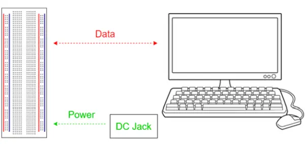
1.2 Visual Aid
High-level requirements list
● The equipment possesses the ability to both read and write logic values at either 3.3V or 5V across every row of the breadboard.
● This device demonstrates compatibility for communication with a host PC via USB 2.0.
● Users can configure the device settings and obtain data from the breadboard utilizing a command line interface.
2. Design
2.1 Block Diagram
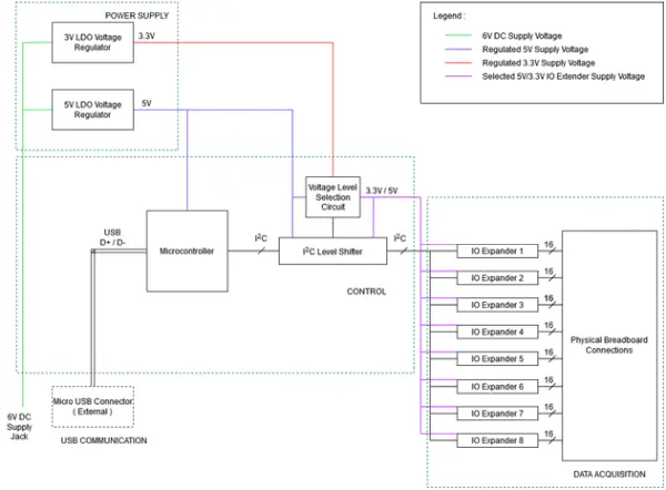
Physical Design
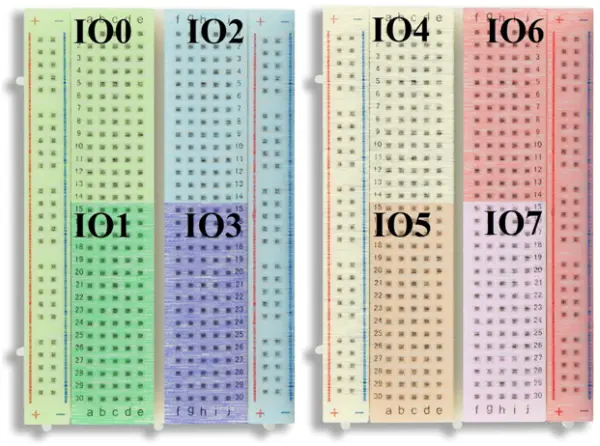
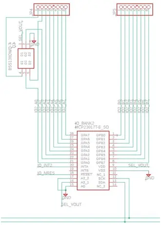
The provided illustration depicts our device’s physical layout. Each IO expander corresponds to a section equivalent to a quarter of the rows on each breadboard, summing up to a total of 8 IO expanders spanning two breadboards. On each breadboard, two IO expanders are allocated specifically for toggling connections to the supply voltage and ground, managing the power rails, rather than directly reading or writing logic values to the breadboard rows.
These IO expanders’ function doesn’t involve reading logic values from the power and ground rails; instead, they facilitate establishing or interrupting connections between the power and ground rails and the supply voltage and ground for the device. This configuration grants flexibility, allowing the usage of these rails as either power rails or bus lines, provided the power supply connections are inactive. This design decision was deliberated to enable a higher current draw from the supply rails, albeit at the trade-off of the inability to directly retrieve values from any signals wired to the supply lines by the users.
Block Level Descriptions
The setup involves attaching the device to the back of two 400-tie modular breadboards [1], thereby establishing connections between the metal rails situated on the breadboard’s rear and a consolidated PCB encompassing all design elements. Each of these rails connects to a line on one of the eight IO expanders in our design. This configuration enables the device to interface with individual signals within the logic circuit on the board, allowing for the reading and writing of logic values in each corresponding row. Figure 3 depicts a standard 400-tie breadboard where our PCB would be affixed at the back to access signals in each row.
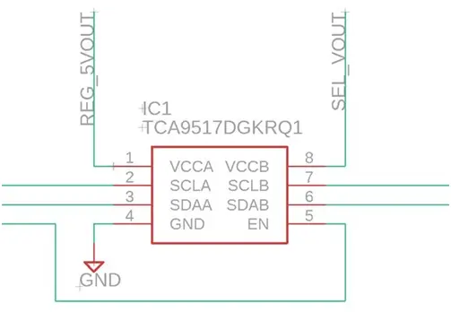
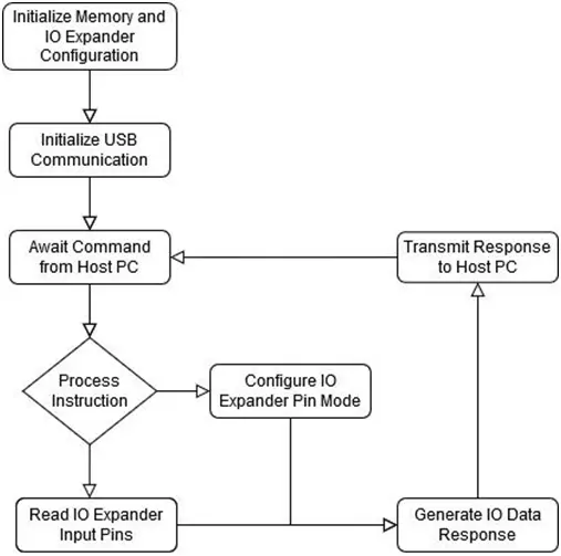
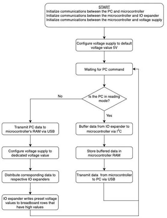
Our device can be compartmentalized into four distinctive blocks, each designed with specific functionalities to facilitate signal reading and writing on a breadboard. Initially, the control block comprises two key elements: a microcontroller and an I2C Level Shifter. The microcontroller oversees the level shifter’s operations, which in turn manages signals from the IO expanders within the Data Acquisition block through I2C. Additionally, the control block integrates a voltage level selection circuit responsible for distributing required voltage values to dedicated IO expanders. Secondly, the power supply block serves the crucial function of supplying power to respective components. Thirdly, the Data Acquisition block encompasses multiple IO expanders externally linked to our breadboard, dedicated to reading and writing voltage values. Lastly, the USB Communication block establishes an external connection to a host PC, facilitating user interaction with our device.
Control
Block Requirement: The control block is responsible for overseeing data acquisition and configuring various peripherals for functions such as USB communication, voltage selection, and data acquisition processes.
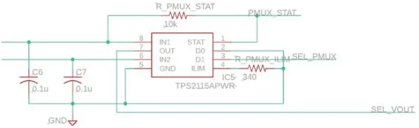
This block will comprise an ATmega32U4 microcontroller, facilitating communication with the host PC via USB and interacting with the data acquisition block through I2C. Additionally, it will utilize a single wire to command a voltage selection circuit, setting the operational voltage for the IO expanders. Operating at 5V from the power system’s regulated 5V supply, the microcontroller requires a level shifter between itself and the I2C peripheral devices due to the need to operate at multiple voltages.
Moreover, the control system will interpret instructions and configuration data received from the host PC, appropriately configure the necessary peripheral devices, capture requested data, and transmit it back to the host PC. This entire process will be managed by the device upon the request of the host PC.
| Requirements | Verifications | Points (15) |
| Microcontroller
1) Process instructions and communicate with the PC |
Verification Process:
1. Communication Verification a) Obtain a multimeter. b) Configure a predetermined output state for IO Expander pins. c) Place ends of multimeter at each predefined row and ground. d) Verify that each row holds its corresponding logic value, as defined in the microcontroller software. 2. Voltage Verification a) Obtain a multimeter. b) Place ends of multimeter at output and ground. c) Ensure supply voltage difference is 5V with an allowed variation of 10% greater and 10% lesser (4.5 to 5.5V range) |
10 |
| Voltage Selection Circuit
1) Switch between an operating voltage of either 5V or 3.3V |
Verification Process:
1) Voltage Verification a) Set voltage selection circuit to for 5V b) Obtain a multimeter c) Place ends of multimeter at output and ground d) Ensure voltage difference is 5V with an allowed variation of 10% e) Repeat for 3.3V |
5 |
Table 1. Requirements and Verification for Control System
Power System
Block Requirement: The power block must deliver both 5V and 3.3V to the device while ensuring sufficient current capacity for all components.
The power system will comprise two distinct power circuits designed to supply the board with dual voltage levels: one set at 5V and another set at 3.3V. Each of these power circuits will be composed of a dedicated voltage regulator along with its necessary components, including capacitors and resistors.
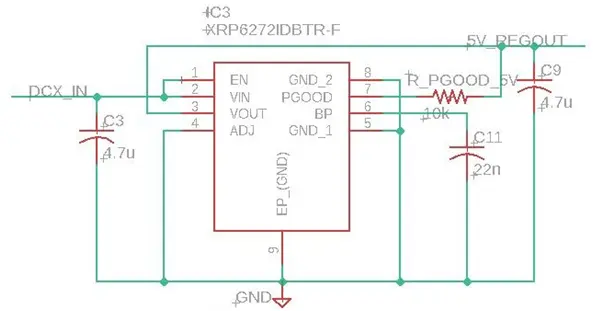
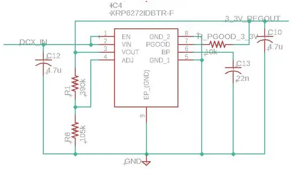
The voltage regulators receive an input voltage and deliver a distinct output voltage. One of the regulators is designated to provide a 5V output, while the other is intended for a 3.3V output. It is crucial for the component used in the first regulator, which produces an output identical to the input, to be a low dropout regulator. Additionally, these components must possess a substantial current tolerance since the circuit experiences a relatively high current flow during peak usage.
| Requirements | Verifications | Points (10) |
| 5V Power Circuit
1) Provide voltage at 5V +/- 10% 2) Supply a maximum of 2 A |
Verification Process:
1) Voltage Verification a) Obtain a multimeter b) Place ends of multimeter at output and ground c) Ensure voltage difference is 5V with an allowed variation of 10% 2) Current Verification a) Obtain a multimeter. b) Probe current of power supply with equivalent load resistance of ~2.5 ohms. c) Ensure current is within 1.7-2.0A range. |
5 |
| V Power Circuit
1) Provide voltage at 3.3V +/- 10% 2) Supply a maximum of 2 A |
Verification Process:
1) Voltage Verification a) Obtain a multimeter. b) Place terminals of the multimeter at output and ground. c) Ensure voltage difference is 3.3V with an allowed variation of 10%. 2) Current Verification a) Obtain an multimeter b) Probe current of power supply with equivalent load resistance of ~1.7 ohms. c) Ensure current is within 1.7-2.0A range. |
5 |
Table 2. Requirements and Verification for Power System
Data Acquisition
Block Requirement: The system should possess the capability to execute digital read and write functions at both 3.3V and 5V for every row available on the breadboard, as directed by the control block.
The data acquisition segment comprises eight IO expander ICs that interface with the microcontroller within the control block via I2C. These IO expanders must function at either 3.3V or 5V and communicate with the microcontroller using the corresponding operating voltage. To facilitate this, a high-speed bidirectional I2C level shifter is employed, specifically designed for I2C applications. This setup enables the microcontroller to consistently operate at 5V while allowing peripheral devices to function at a user-defined voltage. Each IO expander establishes 16 connections to individual rows on the breadboard, enabling read and write operations on any specific row. Furthermore, the power and ground rails can be linked to the logical high voltage and ground correspondingly, or they can be detached from the power supply to function as standard bus lines.
| Requirements | Verifications |
| IO Expanders
1) Read and write 5V and 3.3V voltage values to the breadboard |
Verification Process:
1) Voltage Verification a) Obtain a multimeter. b) Set IO Expander to write 5V c) Place terminals of the multimeter at row and ground. d) Ensure it is 5V with allowed +/- 10% variation. e) Repeat with 3.3V f) Repeat for each IO Expander. |
Table 3. Requirements and Verification for Data Acquisition
USB Communication
Block Requirement: The device should possess the ability to both transmit and receive data with a host PC.
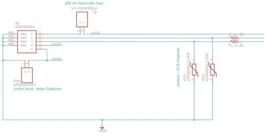
The USB block establishes communication with the PC through a standard USB 2.0 interface. To facilitate effective communication between the host PC and our breadboard, we plan to employ the open-source library libusb [2] for managing USB communication with the microcontroller. This library streamlines hardware communication without requiring additional processes like creating a dedicated kernel. Opting for libusb presents numerous advantages. Firstly, it is an actively maintained open-source library accessible through online forums, offering support to users. Secondly, it boasts compatibility across various platforms such as Windows, IOS, Linux, among others. Thirdly, libusb supports multiple programming languages, making it an ideal fit for our educational breadboard, accommodating diverse operating systems and coding environments suitable for beginners from varied backgrounds.
Our design focuses on synchronously transferring I/O data between our device and the PC. Synchronous device I/O was chosen considering the modest data volume of 257-bits via USB 2.0. This data can be segregated into three segments: 128-bits representing the voltage rows’ values; 128-bits indicating the read/write mode of each breadboard row; and the last bit configuring the reading voltages of the IO expander (3.3V or 5V). Given the single device dealing with 257-bits of data, synchronous transfer proves to be the most efficient method [3].
Furthermore, creating a Python library atop the microUSB controller is imperative. This library will encompass functions for initializing USB communication, configuring the device’s state, updating breadboard data, and retrieving data values. Additionally, the library will parse the data into a readable format, enabling users to conveniently specify the breadboard rows for writing operations.
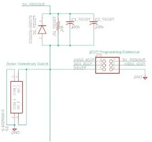
The MicroUSB circuit, depicted below, draws inspiration from the hardware design of the Arduino Leonardo schematic [4], utilizing the same ATmega32U4 microcontroller.
| Requirements | Verifications | Points (15) |
| microUSB
1) Synchronously read data from the microcontroller to the PC 2) Synchronously Write 5V from the PC to microcontroller |
Verification Process:
1) Reading Verification a) Store ‘10101010’ in the ATmega32U4 microcontroller’s RAM b) Using usblib in Python, pyusb, to perform control_transfer() [5] c) Set all function parameters according to data sheet from ATmega32U4 d) Specifically, check bmRequestType parameter is set read e) After calling, make sure that ‘10101010’ shows on the PC 2) Writing Verification a) Using usblib in Python, pyusb, to perform control_transfer() [5] b) Set all function parameters according to data sheet from ATmega32U4 c) Specifically, check bmRequestType parameter is set write d) Set data parameter to ‘01010101’ e) Ensure we receive ‘01010101’ in ATmega32U4 microcontroller’s RAM |
15 |
Table 4. Requirements and Verification for USB Communication
Tolerance Analysis
The functionality of USB transfer stands as a pivotal aspect for the success of this project. Given our limited collective experience in USB communication, we identified USB data transfer as the most significant risk to the project’s completion. To address this crucial block, we opted to employ the open-source library libusb for facilitating USB communication between the host PC and our device. In libusb, two primary methods for device I/O transfer exist: synchronous and asynchronous.
Typically, when the host reads from the device, it involves sending a data request to the device followed by receiving the requested data by the host. Conversely, when the host writes on the device, it entails sending data to the device, with the host receiving a signal indicating the process’s success. The distinction between synchronous and asynchronous methods lies in the number of function calls utilized. Synchronous methods involve a single function call for the above steps, simplifying the process as the call notifies the host about the transfer’s completion. On the other hand, asynchronous methods require two separate function calls for reading or writing, enabling communication with multiple endpoints but escalating complexity.
Considering our device involves handling a single device and a single data array, we opted for synchronous I/O transfer. Our usage of USB 2.0 full-speed, operating at a rate of 12±0.24 Mbits/s or approximately 1.5 MB/s [6], aligns with our data transmission requirements, given the total data size between the PC and the device amounts to 257-bits. However, potential issues could arise, such as the inability to cancel a request once sent and the blocking nature of synchronous calls, which would pause the application within the libusb function until the transfer concludes. This means that if one of our IO Expanders fails to respond, the command line on the PC would freeze without displaying any error messages.
The transfer speed of USB 2.0 sufficiently accommodates the maximum data capacity from the IO Expanders, even when operating at the microcontroller’s maximum possible speed. The complete I2C data request framework is illustrated in Figure 13 below: [Insert diagram here]
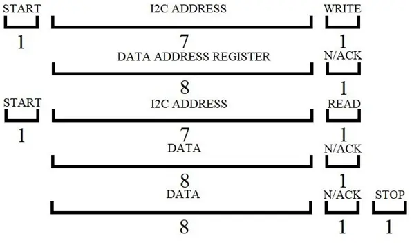
This framework necessitates 47 clock cycles to execute a complete 16-bit read from each IO expander. Acquiring data from each IO expander totals to 47 * 8 = 376 clock cycles for reading from each IO expander. Leveraging the microcontroller’s highest achievable I2C clock speed of 1MHz, this establishes the maximum theoretical frequency for a full-board read at approximately ~2.79 kHz, equating to a total duration of 358.85μs. Considering each transfer accommodates a maximum of 120 bits of data (16 IO pins * 8 IO expanders), the data transfer rate for the IO expander block reaches 334 kb/s. This rate falls significantly below the USB 2.0 full-speed standard of 12Mbit/s and will persist as the bottleneck in read operations.
3. Differences
Overview
The original project, titled the Educational Smart Breadboard [7], was initially conceived by Chinemelum Chibuko, Minseong Kim, and Mostafa Elkabir in Spring 2018. Their creation was an independent device capable of extracting voltages from the breadboard rows and showcasing them on an integrated touchscreen display. Their design segmented the entire breadboard into 8 distinct sub-boards, managed through a hierarchical tree mux structure, and included a dedicated space for chip testing. In contrast, our design focuses on reading and writing logic values in each breadboard row utilizing IO expanders and a microcontroller via I2C. This setup enables configuring the breadboard’s state, communicating back to a host PC, allowing users to adjust inputs and observe logic circuit outputs.
Our approach to addressing challenges associated with debugging intricate breadboard circuits diverges from the original design in several key aspects. Firstly, instead of integrating multiplexers, our design employs IO expanders. This modification grants us the ability to not only read specific sections but also write to individual rows on the breadboard. Consequently, there’s no requirement for a dedicated chip testing region, as our entire breadboard can fulfill this functionality. However, the drawback here is our design’s inability to read analog signals.
Secondly, we opted to forego the standalone touchscreen feature in favor of a device configurable via USB 2.0, establishing connectivity with a PC. This alteration allows users to conveniently configure the device through usblib, enhancing their command line experience.
Analysis
The original project’s architecture relied on a hierarchical tree muxing structure at the heart of its data acquisition system. This structure empowered their ATmega328 microcontroller within the processing block to choose a specific sub-board on their breadboard apparatus [8]. By muxing the breadboard rows into a set of shared pins on the microcontroller, the initial design enabled direct reading of analog values from the breadboard via the microcontroller’s ADC pins.
However, this approach confined the microcontroller to handle only one sub-board at a time, disconnecting all other unselected sub-boards. This limitation severely curtailed testing capabilities for intricate logic circuits, restricting their design’s chip testing functionality to “stable input-output relationships allowing for a fixed truth table” [7]. Such constraints hindered users from leveraging the testing functionality for more complex circuits like register ICs or FSM circuits. In contrast, our adoption of IO expanders eliminated this limitation. Our design could write logic values to any combination of breadboard rows concurrently. This feature enabled the testing and debugging of various ICs or logic circuits where specific inputs should yield known outputs, such as with register ICs or FSM circuits. This difference significantly enhances the functionality of our device, maximizing its utility for debugging, testing, and verification applications.
Although utilizing IO expanders restricted us to reading solely digital logic values from the breadboard, we deemed this non-critical for two reasons. First, entry-level users likely testing analog circuits on a breadboard might have fewer crucial test points for debugging, reducing the necessity for a more complex device like ours. Conversely, digital logic circuits often possess a high degree of complexity, benefitting from numerous test points for debugging, aligning with our priority on digital circuit utility. Second, the voltage range for simple ADC ICs imposes limitations on the maximum voltage applicable to breadboard rows. This restricted voltage tolerance limits the range of analog values present on the breadboard without endangering sensitive components. In contrast, digital logic circuits, functioning within supply voltages < 5V (the range of our microcontroller and IO expanders), are less affected by these voltage tolerance limitations.
The second crucial difference pertains to user-device interaction. The original project aimed for a standalone device employing a touchscreen display for user configuration and data output. This approach constrained automated testing and verification as it required users to input the complete truth table for the logic circuit or IC into the touchscreen display to conduct tests. However, by transforming the device into a USB peripheral, enabling user configuration and data retrieval through a Python library, we grant users greater operational freedom. This shift allows for automated testing and verification using a code library. Additionally, it facilitates FSM testing by enabling the setting of circuit inputs and direct measurement of resulting state changes without extensive probing. This departure from the touchscreen display significantly amplifies our device’s utility while simultaneously reducing costs by eliminating an expensive component.
- What is the primary function of the Smart Breadboard?
The device reads and writes digital logic values on every breadboard row and communicates with a host PC for configuration and data exchange. - How does the Smart Breadboard communicate with the host PC?
It communicates via a USB 2.0 interface using libusb and a Python library for synchronous transfers. - Can the device operate at different logic voltage levels?
Yes, it can switch between 5V and 3.3V using a voltage selection circuit and appropriate regulators. - How many IO expanders are used and what is their role?
Eight IO expanders are used; each provides 16 connections to rows for digital read and write operations. - Does the Smart Breadboard read analog signals?
No, the design reads only digital logic values and does not support analog readings. - Why is a level shifter needed in the design?
Because the microcontroller operates at 5V while IO expanders may operate at 3.3V or 5V, a bidirectional I2C level shifter lets them communicate safely. - What data is transmitted between the PC and device each transfer?
257 bits total: 128 bits for row voltage values, 128 bits for read/write mode per row, and 1 bit for IO expander voltage selection. - What verification method is used for USB read/write?
Using libusb in Python (pyusb) control_transfer calls to read/write known bit patterns between PC and the ATmega32U4 RAM. - How is power provided to the device?
Two dedicated regulator circuits supply 5V and 3.3V, each designed to supply up to about 2 A and include necessary passive components. - What advantage do IO expanders provide over the original mux design?
IO expanders allow concurrent reading and writing to any combination of rows, enabling testing of complex digital circuits without the one-sub-board-at-a-time limitation.