Summary of Green Charger
The Green Charger is a portable solar-powered phone charger with a UV detector and TFT display. It uses two 2.5W solar panels, buck/boost converters, and an LDO to supply 5V for USB charging and 3.3V for a PIC32 MCU. The MCU reads voltages and UV sensor output via ADCs, displays voltages, charging progress bars, and UV-based advice on a TFT, and is controlled via a 12-button keypad. Design prioritized portability, RoHS compliance, and budget constraints; future work includes precision current sensing and improved enclosure and wiring.
Parts used in the Green Charger:
- PIC32 microcontroller (Microstick PCBA)
- Adafruit TFT display
- Two ALLPOWERS 2.5W 5V 500mA solar panels
- Adafruit Verter 5V buck/boost converter
- LD1117 LDO (3.3V regulator)
- Analog UV Light Sensor Breakout - GUVA-S12SD
- 12-button keypad
- USB-A female connector (power only)
- 10 μF capacitors for LDO
- 10kΩ resistors (voltage dividers)
- 330Ω resistors (keypad row resistors)
- Wires, solder, plywood mounting board
Introduction
Have you ever gone to the beach on a hot summer day with your family only to complain that your phone is so low on battery that you can’t even take a selfie? Have you ever been concerned that you’re not putting on enough sunscreen, or sunscreen that isn’t strong enough? Have you always wanted to play a part in protecting our planet?
Well, we have a product for you! Introducing the GREEN CHARGER a product that can solve all of those problems and provide an environmentally friendly alternative to traditional portable chargers!
High Level Design
Rationale and Sources for Project Idea
The initial idea of the project comes from the group members’ collective interest in green energy. Climate change is a widely discussed topic and there has been much debate on how humans should try to mitigate the impact of climate change. Thus, we would like to create a sustainable product that uses clean energy and helps to reduce the usage of non-renewable and pollutive energy sources such as fossil fuels. As such, we decided to build a portable solar cell phone charger to utilize sustainable and renewable solar energy.
The main feature of this project will consist of two solar cell panels that will utilize light energy to produce electrical energy. It will be designed and built to have multiple purposes based on the power output from the solar cell panel. This project will consist of 2 main functionalities that will be implemented in the order that they are described.
The first purpose of this project is to be able to charge a phone with the electricity generated from the solar cell. Using the microcontroller, we aim to display the voltage output from the solar cell on the TFT display.
The second functionality of our project includes a UV detector. We used a UV sensor as our UV detector, which outputs an analog signal in relation to the amount of UV light that’s detected. Using the ADC on the PIC32, we can convert the analog signal to a digital input which will tell us how much UV light is present. Based on the information provided in the datasheet of the UV sensor, the analog voltage can be directly converted into UV index. Based on this information, we can display a warning to the user to inform him/her that there is too much UV light present. Advice will be displayed on the TFT screen to tell the user what is the appropriate course of action to take.
Background Math
All mathematical equations used in this project will be discussed in detail in the Software section. The mathematical equations used are relatively straightforward.
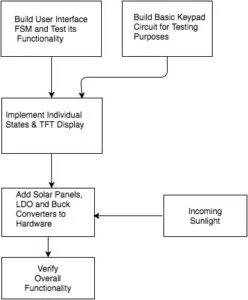
Logical Structure
The following diagram demonstrates the logical structure of our entire system:
Hardware and Software Tradeoffs
Due to a limited number of ADC pins that were available on the microcontroller, space constraints on the breadboard (our system has to be portable) and budget constraints, we were not able to construct additional hardware to measure the full IV characteristics of the power and current being supplied by both the solar panels. Fortunately, the problem of computing the IV characteristics was mitigated by having the software display the voltage characteristics of the cell phone charger and the voltage being supplied to the microcontroller with the help of the ADC pins that were available. This was sufficient in helping us debug as well as providing useful information for the user to determine an estimate of the power being supplied to both the MCU and the cell phone.
Standards
We have followed the following standards from IEEE and ISO while implementing the project. All parts are RoHS compliant.
IEEE SCC21 specifies uniform standards in the development of fuel cells, photovoltaics, dispersed generation, and energy storages. It also contains the performance, testing and safety considerations of the electric power systems.
ISO 50001: 2011 specifies the standards of implementing and improving an energy management system and help improve energy performance.
We also followed the standards for Restriction of Hazardous Substances (RoHS). Also known as directive 2002/95/EC, this policy originated in the European Union in an effort to restrict specific hazardous materials found in hazardous products. The USA is adopting these standards.
Related Copyrights and Existing Patents
This project idea was a product of a brainstorming session by the group members and the final product was designed and built by ourselves from scratch. There are no known patents or copyright issues associated with this project.
Program/Hardware
Hardware Details
The hardware of the Green Charger consists mainly of a PIC32 microcontroller, a TFT screen, 2 solar panels, buck converters and an LDO. The schematic for connecting all the modules together are depicted in the Appendix below.
Solar Panel
Our starting point for all our hardware decisions was based on what types of photovoltaics we would use. After some research, we found that PV cells with a high current would be fairly costly. Since we did not have a large enough budget to spend upwards of 40 or 50 dollars on a high power (wattage) solar cell, we opted for a cheaper one that would meet the voltage specifications while only sourcing low amounts of current. This is most problematic for the phone charger itself, as phones charge more quickly when more current is supplied. However, as long as the voltage specification is met, the phone will charge. As for the MCU, we roughly estimated that in steady state it would draw no more than ~200 mA of current, and this was a rough estimate. Nevertheless, we picked components that could supply it much more.
We used the two 2.5W 5V 500mA ALLPOWERS solar panels. They were sized 130×150 mm, so they were neither too big nor too small for the project. After doing some research on the part, we learned that the OC voltage could be as high as 8.2V, and on sunny days the voltage (with a load circuit) could still go as high as 6V. In addition, the current almost never actually reached 500 mA. More often than not, it would stay around 200-300mA on sunny days. This prompted us to look for a buck converter that could step down the voltage to a safe 5V value for our USB connection and for another buck converter that could safely step it down to 3.3V for our MCU.
Buck/Boost Converter
However, there were two problems with the approach described above. First, on days with less sun, the voltage produced from the solar panel may be slightly lower, around 4.5V. Second, a buck converter’s switching would add noise onto the MCU power line, which could lead to problems in the digital logic computations on the chip, or even worse–if the noise was large enough–cause the MCU to shut down if the voltage exceeded its maximum and minimum bounds.
To solve these problems, we decided to use a buck/boost converter which could handle a range of input voltages and still maintain a constant output voltage. We used Adafruit’s Verter 5V buck/boost converter to do just this. For the USB charger, we simply soldered a USB-A female connector to it, only connecting the power pins to the board. All data pins were left floating, as no data is being transmitted. For the MCU, we decided to connect a LDO in series with the buck/boost converter, and use the output of the LDO to power the MCU.
The buck/boost converter specifies an input voltage of 3V to 12V, an output voltage of 5V, and a current of up to 500 mA in boost mode, and up to 1000 mA current in buck mode. For reference, most USB phone chargers will supply 500 mA at 5V (2.5W). With USB 3.0, this has been increased to 900 mA, and dedicated USB charging ports can go as high as 1500 mA. Wall chargers that are provided when purchasing phones can go even higher; Avi’s motorola charger provides up to 2.85 A. However, these high current values were infeasible for this project, and were even higher than what a user would experience when plugging in their phone to their laptop or personal computer to charge.
With these details in mind, we initially decided to connect the solar panels in parallel, and load the regulated +5V line with both the MCU (after connecting it to the LDO) and the phone charger. However, when tested, the phone charger sunk all of the current, causing the MCU to shut down. Since we did not have any fancy current control mechanisms, we simply decided to isolate the two circuits of the solar panels.
LDO
At this point, the final piece of hardware to finalize was which LDO we needed to use. This wasn’t a hard decision: all we needed was something that had specified an input voltage of 5V and an output voltage of 3.3V, regulating current up to 500mA. At the time of the decision, we were not sure if the panels would be in parallel or not, since we had to order all parts in the beginning. We found a small, elegant solution in the form of the LD1117. This through hole LDO was rated up to 800mA, cost less than $2, and was very easy to work with.
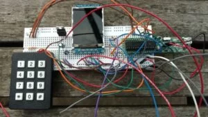
KeyPad and TFT
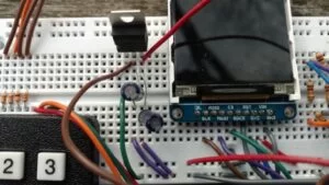
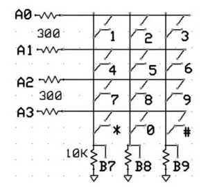
The hardware design for the TFT and keypad was straightforward in its setup but complicated in its implementation. First, we connected the adafruit TFT display to the microcontroller using the suggestions from the ECE 4760 lab 2 website. That is, for the TFT display, SCK1 is connected to RB14 (pin 25) on the PIC, MOSI (SDO1) is connected to RB11 (pin 22) on the PIC, CS is connected to RB1 (pin 5) on the PIC, RST is connected to RB2 (pin 6) on the PIC, D/C is connected to RB0 (pin 4) on the PIC, and VIN is connected to 3.3V supply. Finally, we connected the 12 button keypad to the microcontroller via the A0 (pin2), A1 (pin 3), A2 (pin 9), A3 (pin10), B7 (pin 16), B8 (pin 17), B9 (pin 18) pins. For pins B7, B8, and B9, we enabled the 10k internal pulldown resistors to lower the drive current via the software implementation. That is, setting CNPDB = BIT_7 | BIT_8 | BIT_9 in the keypad thread pulls down B7, B8, and B9. Also, on pins A0 through A3 we placed 330 ohm resistors to lower the drive current. A detailed keypad connection scheme is shown in Figure 5 and was borrowed from ECE 4760 lab website.
Putting It All Together
With all the hardware ordered, we tested it with some loose connections and only a few components soldered, and then once we finalized the layout, we began the physical construction.
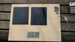
We used an approximately 12” x 18” x 0.25” plywood board to mount our solar panels. We drilled 0.375” holes into the board: 2 for the PWR and GND connections of Solar Panel 0, 2 for the PWR and GND connections of Solar Panel 1, 2 for the breakout board with the USB connection, 4 for the breakout board routed to the MCU, and 3 for the UV detector (13 in total). We soldered copper wires to all the ports we needed to, and then physically routed it through the drilled holes. We used tape on the back of the solar panels and breakout boards to keep them in place on the wood, however wood glue could be used instead for the solar panels. Once this was done, on the backside we taped wires down to prevent them from getting messy, and soldered the remaining connections we needed. While this form of soldering was not the cleanest or most robust, we deliberately did not do anything that would be more difficult to undo since the project was an iterative process that required a lot of testing and debugging along the way. We would have ended up spending significantly more time had we gone and gotten a solder board, soldered connections to it, removed connections to it, etc. By simply soldering wires directly together, we saved a lot of time. However, if we were to market this as a product, we would definitely have more stable and professional connections. Finally, we routed the loose copper wires away from the board to connect to the MCU. Again, if we moved to market this product, we would probably replace these loose wires with a bundled connection to make the project neater.
Finally, we needed some additional wires from the solar panels to the MCU. We soldered two wires, one on each voltage rail of each panel. These wires were used for the ADCs of the MCU to measure the voltage characteristics.
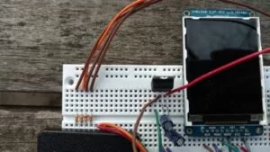
For the MCU, we chose to stick with the breadboard for easier debugging and so we could move things around. We opted to use the Microstick PCBA since none of us wanted to waste time understanding the schematic required to operate the MCU (i.e. the resistors, capacitors, and transistors needed to operate the clock, regulate voltages, etc). By leaving the microstick in, we were able to easily program the MCU as we had done in previous labs. Had the MCU drive circuitry been another of our subsystems, it would have cost us more time in debugging.
Finally, we needed some additional wires from the solar panels to the MCU. We soldered two wires, one on each voltage rail of each panel. These wires were used for the ADCs of the MCU to measure the voltage characteristics.
For the MCU, we chose to stick with the breadboard for easier debugging and so we could move things around. We opted to use the Microstick PCBA since none of us wanted to waste time understanding the schematic required to operate the MCU (i.e. the resistors, capacitors, and transistors needed to operate the clock, regulate voltages, etc). By leaving the microstick in, we were able to easily program the MCU as we had done in previous labs. Had the MCU drive circuitry been another of our subsystems, it would have cost us more time in debugging.
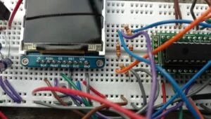
The Microstick connected to a computer/laptop with its own mini USB connection, which was used for programming the MCU. While this connection was maintained, the MCU received its 3.3V power, thanks to the Microstick. However, the design of the project is so that when the customer would receive this, there would be no USB connection on the microstick that they could connect to. Instead, all 3.3V would be generated from the solar panel. See Figure 4 for a close up connection of the LDO.
For the LDO, we needed to supply it with capacitors to store charge. The LDO is an arrangement of transistors (essentially), and in order for it to function well, as it switches it needs to draw and deposit charge fast. The 10uF capacitors do exactly that. Polarized capacitors make no difference as the voltage is never negative on the LDO.
The last section of hardware was the voltage dividers for the ADCs. Since the voltage could go as high as 6V under sunlight, we decided to use two 10K resistors to halve the voltage down. Then, in software, we multiplied the value by 2 to get an accurate reading of the voltage. See Figure 8 for a close up of the voltage dividers.
Program/Software Details
We have used a finite state machine for the overall user interaction with the solar charger as well as the UV detection. The state transition of the finite state machine is shown in Figure 9. We have organized the various states for the solar cellphone charger in a finite state machine. Upon entering the charger, we have a state 0 where a welcome message is printed. The next state is the main menu where all the states are listed and the way to get to each state is also specified. Thus, according to the specification, the user can press the corresponding keys to go to the desired states.
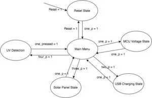
We also decided to include a pictorial representation of the voltage being supplied to the MCU. This allows the user to view the voltage being supplied to the MCU and enhances the quality of our display. This is shown in the form of a progress bar, which increases in length as more voltage is being supplied to the phone. The implementation of the progress bar is explained in greater detail in the USB charging state.The detailed states going from the main menu and their functionalities are listed below.
User interface :
The TFT display used here is mainly used for the user interface.
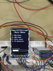
The four modes are MCU voltage, USB charging, Solar panels’ voltage and UV detection.
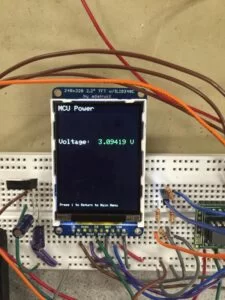
MCU voltage state :
The purpose of this state is to display the voltage supplied to the MCU and the user can see the voltage provided to the microcontroller by pressing 1 once it is in the main menu. By configuring an ADC pin (pin 26) on the MCU, we were able to measure the voltage supplied to the MCU. A digital reading which is obtained from the ADC is then converted to a voltage with a simple equation:
( Vref*adc_reading/1023 ) * 2 = voltage supplied to MCU
In this case, the voltage reference we are using is 3.3V since the ADC is only able to measure up to 3.3V. It is also important to note that we have a multiplication factor of 2 in our equation. This is because we are using a voltage divider circuit which consists of two 10K ohm resistors. Since the voltage could go as high as 6V under sunlight, it was necessary to use two 10K resistors to halve the voltage down. Then, in our code, we multiplied the value by 2 to get the correct reading of the voltage supplied to the MCU.
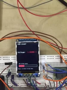
USB charging state :
This state is used to display the voltage supplied by the other solar panel to the phone and the user can observe the voltage provided to the cell phone by pressing 2 once in the main menu. As described in the MCU voltage state, we reused the same equation to determine what is the voltage that is supplied to the phone. By configuring another ADC pin (pin 7) on the MCU, we were able to measure the voltage supplied to the cell phone. A digital reading which is obtained from the ADC is then converted to a voltage with the same equation as described in the previous section.
Furthermore, in addition to a numerical value being displayed on the TFT screen, we also decided to include a pictorial representation of the voltage being supplied to the cell phone. This allows the user to view the charging status of the cell phone. This is shown in the form of a progress bar, which increases in length as more voltage is being supplied to the phone. The colour of the progress bar also changes based on how much voltage is being supplied to the cell phone. The maximum length of the progress bar is 210 pixels and the length of the progress bar is determined by performing a linear scaling based on the voltage measured. The colour red indicates that a low voltage is being supplied to the cell phone and thus, the cell phone will take a long time to charge up. The colour yellow indicates that the cell phone is being charged at a moderate rate. The colour green indicates that there is a generous amount of voltage that is currently being supplied to the cell phone and it will take a short time to charge the cell phone to full power. To remove flickering of the progress bar, the voltage is continuously monitored and as long as the voltage does not change, the progress bar does not update. In other words, the progress bar is only redrawn whenever a change in voltage has been detected.
Solar Panel state :
This state display the voltages of both solar cell panels and the user can access this state to read the voltages provided by each solar panel by pressing 3 once in main menu. As described in the MCU voltage state and the USB charging state, we configured the same ADC pins (ADC pin 7 and ADC pin 26) to measure the voltage that is supplied by the solar panels. This was relatively straightforward as we just had to reuse the connections and equations that we had used in the USB charging state and the MCU voltage state. The numerical values of the voltages supplied are then displayed on the TFT screen.
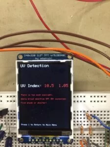
UV detection state :
This state measures and display the current UV index and the user can access this state to read the current UV index and take actions accordingly by pressing 4 once in main menu. Advice is also provided for the user to determine what is the correct course of action to take and the course of action depends on the amount of UV light detected by the Analog UV Light Sensor Breakout – GUVA-S12SD. An additional ADC pin (pin 26) has been configured on the MCU to measure the voltage output from the UV detector. The sensor is powered with 3.3V by the MCU and it shares the same ground as the MCU. Using the following equation, we can obtain the output voltage from the UV detector:
( Vref*adc_reading/1023 ) = output voltage from UV detector
In this case, the voltage reference we are using is 3.3V. No voltage divider was used for the output voltage, thus there is no multiplication factor of 2 in this equation because the output voltage from the UV detector is expected to be much lower than 3.3V. According to the equation provided by the product’s web page, we can directly convert the output voltage from the UV detector into the corresponding UV index with the following equation:
UV index =output voltage from UV detector/ 0.1
If the output voltage from the UV detector is 1V, then the UV index is approximately 10. Given that the highest recorded UV index in the history of mankind is 26, we can see that the output voltage from the UV detector could theoretically only meet a maximum of approximately 2.6V. The equation for the UV index was obtained from the datasheet. We used the graph (shown below) extracted from the datasheet to compute the UV index from the photocurrent obtained from the UV detector.
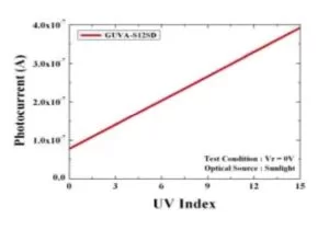
According to the product’s datasheet, the output voltage of the UV detector related to the photocurrent by the following equation:
Output voltage from UV detector = 4.3 * Diode-Current-in-uA
If the photocurrent is 0.2uA, the output voltage is 0.86V, which corresponds to an approximate UV index of 8.6. After obtaining a measurement of the UV index, the next step was to use a UV index scale to determine what advice we should display to the user. We obtained this information from the US Environmental Protection Agency’s webpage https://www.epa.gov/sunsafety/uv-index-scale-1. In our code, we have 4 different levels of UV index. When the UV index is 2.9 and lesser, we display a message that tells the user that there is little or no sunlight available. When the UV index is between 2.9 to 5.9, the TFT display tells the user start applying sunscreen. When the UV index is between 5.9 to 10.9, the TFT display will tell the user to start finding shade or shelter. When the UV index is above 10.9, the TFT display will tell the user that he/she is in grave danger. Similar to how the progress bar is updated, the TFT display only updates the numerical value of the UV index when it changes and the advice is only updated whenever the UV index goes into a different level. This is done using additional variables that store the previous value of the UV index. This approach removes flickering from the TFT display.
Things That We Tried
One major problem we encountered during software implementation was the decision on whether or not to sense the individual current provided by each solar cell panel. After we did some research on the current sensing techniques related to our project, we found that in order to accurately quantify the current, we would need precision inductors as well as operational amplifiers, which would result in additional hardware and software expenses. As we were already very close to the budget limit of $100 that was imposed on the project, the group ultimately decided not to include current and power as part of the TFT display.
Results
Speed:
The overall execution speed was very fast since in software we only had two concurrent threads. One thread is used to kept track of which key is pressed and the other thread allows the user to switch between various states and check the proper functionality and result accuracy of each state. To remove flickering of the progress bar, the voltage is continuously monitored and as long as the voltage does not change, the progress bar does not update. That is, the progress bar is only redrawn whenever a change in voltage has been detected. Charging of the phone takes a longer time if the amount of sunlight is low.
Accuracy:
Depending on the intensity of the sunlight, the amount of current supplied to the phone will vary. The maximum amount of current we observed from the solar panel charging the phone was around 250mA with a multimeter. The charging time to increase the battery power by 10% could be estimated to be around 1 hour for a smartphone with a large battery, or about 20% for a smartphone with a smaller battery. Due to the very limited sunshine present during the winter season in Ithaca, the final product was successfully tested a few times. When the final product was tested on cloudy days, the solar panel that provides power for MCU was not able to get enough power. As a result, the MCU wouldn’t turn on and the cell phone was not able to get charged since there was not enough sunlight for the solar panel to supply enough power.
However, during one of the more successful tests on a partially cloudy winter day, the voltages supplied to both the MCU and cell phone were 4.5V and the UV detection state displayed “Sunlight is not that intense” message on the TFT display since the UV index was only around 0.11. The voltage reading was quite accurate since we measured the voltage again using a multimeter and the variation between the two readings was less than 0.1V. The UV detection worked as expected since the amount of UV present would be low on a cold cloudy winter day. Heat lamps were also used to perform the tests. Three heat lamps were used to provided 4.5V voltages to both the MCU and cellphone. The UV detector worked correctly as well and read an UV index of 0.01, which is consistent with the very low UV emission of heat lamps. Based on these results, we could speculate that the final product will work as expected in the sunny summer days, although it’s unfortunate that this project was carried out during winter season where sunlight is extremely rare.
Safety:
Since there are many hardware implementations in this project, in each step of the hardware design, we double checked our calculations and designs to ensure the circuit would work as anticipated and wouldn’t overload any hardware components. For example, when we were connecting the keypad in the MCU circuit, we enabled three 10K internal pulldown resistors to lower the drive current via the software implementation. Also, for pins A0 through A3 we placed 330 ohm resistors to lower the drive current. Another safety measure was included for the ADCc. Since the voltage from the solar panel could go as high as 6V under sunlight, we decided to use two 10K resistors to halve the voltage down. Then, in software, we multiplied the value by 2 to get an accurate reading of the voltage.
Level of interference:
This project does not cause any interference to other people. It is quiet and clean and there are no radio frequency components that are included in our project.
Usability by others:
The final product of this project exhibits high levels of usability. The user can just connect their phone to the USB port, put the whole setup directly under the sun on a sunny day, and the Green Charger will automatically charge the cell phone and display the appropriate voltage values on the TFT display. The user interface is designed in a way to exhibit the highest levels of user friendliness. The user interface has a redirecting message in each state, and the user is able to conveniently move to the next state with one key press. In addition, we have provided the UV index and the appropriate advice corresponding to the magnitude of the UV index so that the user can be warned of any excessive UV radiation.
Conclusions
Expectations and Future Work
Overall, this was a fun project and we were able to design the final product such that it has all the functionalities we have planned in the project proposal. The final product is able to provide enough power for the MCU using one of the solar cell panel and properly charge the cell phone using the other solar cell panel. The final product can also display the voltages provided by both solar panels on the TFT display and the current UV index so that the user can be advised on the course of action to take with the current UV index. Meanwhile, we didn’t measure the exact current provided by both solar cell panels due to budgetary constraints (i.e. the total budget should be less than $100) on the project.
However, this project can have many different improvements that would increase functionality. If we were to have additional funding, we would have built a precision current sensing circuit for both solar cell panels. In addition, the overall hardware connection takes a lot of space and the keypad and MCU connections on the breadboard is particularly messy. Thus, a possible future effort could be to clean up the hardware connections and make it more professional and appealing to users. As discussed above in the hardware design section, the voltages provided by both solar cell panels are constrained to be within the safe operation region for both the MCU and cell phones. Although the current provided by the phone-charging solar panel is relatively low compared to that of the standard charging techniques such as USB charging via laptops, the solar charger is able to meet the voltage specification and charges user’s cell phone.
Standards
Our project followed the protocols specified by IEEE. We have followed all the IEEE, and ISO standards specified above in the Standards section of High Level Design. All parts of the design are RoHS compliant.
Intellectual Property Considerations
Most hardware and software design were developed and implemented by our group and we borrowed the keypad connections and the basic thread tutorials from previous lab assignments on ECE 4760 website. In addition, we used the PIC32 standard library, plib, as well as the Protothreads library. All of the code was written on our own and no code was used from the public domain. We do not expect our project to be patented. We have properly attributed all references and sources that we have used in the appendix section.
Ethical Considerations
The IEEE Code of Ethics were constantly adhered to throughout the design and implementation of this project.
Our project is consistent with the IEEE Code of Ethics and the detailed explanation is shown below. The solar charger is designed and built for educational purposes to enhance our understanding on the solar panel real-life applications, improve our project management skills by building a functional and efficient product with limited time and budget, and further help improve our software programming skills using PIC32 microcontroller. This project doesn’t pose any threat to the “safety, health, and welfare of the public.” If future safety concerns are discovered, they will be resolved and reported to the public immediately. During every step of the project implementation, all group members have made sure that the product is safe both in design and in practice. For the software implementation, we have made sure that all source code and libraries are acknowledged properly and if anyone else identifies problems in the code implementation, we will make the necessary change and update the public as well. In addition, all resources and references are cited properly to acknowledge the intellectual ownership of others. This project treats everyone as equals and doesn’t discriminate any person based on their sociological background, and it does not pose any “conflicts of interest”.
Source: Green Charger
- What is the primary function of the Green Charger?
To charge a phone using two solar panels while displaying voltages and UV index on a TFT driven by a PIC32 MCU. - Can the Green Charger display the voltage supplied to the MCU?
Yes; the MCU measures its supply via an ADC and displays the computed voltage on the TFT. - How does the Green Charger determine UV index?
The GUVA-S12SD UV sensor output voltage is read by the MCU ADC and converted to UV index using UV index = output voltage / 0.1 based on the sensor datasheet. - What power regulation components are used for USB and MCU power?
An Adafruit Verter buck/boost converter provides 5V for USB and an LD1117 LDO provides 3.3V for the MCU. - Does the project measure solar panel current or power?
No; current and power measurements were not implemented due to budget and hardware constraints. - How does the user interact with the Green Charger?
Via a 12-button keypad and TFT menu with four modes: MCU voltage, USB charging, solar panel voltages, and UV detection. - What safety measures were implemented for ADC voltage readings?
Two 10kΩ resistors form a voltage divider to halve solar panel voltages so ADC inputs stay within 3.3V limits. - Can the Green Charger charge phones in low sunlight?
Performance depends on sunlight; on cloudy days panels may not supply enough power and charging may be slow or fail. - What displays indicate charging status?
A progress bar on the TFT represents the voltage supplied to the phone and changes color by voltage level.