Summary of Microcontroller-Driven AC Voltage Control with Soft Start Feature
Summary (under 100 words): This project implements a microcontroller-based PWM AC voltage controller using anti-parallel SCRs with optocoupled gate drives, phase and frequency synchronization, and RMS feedback for stable output. Two AVR microcontrollers (ATmega32 for PWM/synchronization and ATmega8 for RMS measurement) coordinate interleaved PWMs, PID-based feedback, and a lookup table to derive firing angles/duty cycles. Prototype testing on resistive loads shows nonlinear power control, efficiency rising with load, and increased harmonics at firing angles above 90°, recommending operation at or below 90° or using filtering/adaptive range selection.
Parts used in the SCR-based AC Voltage Controller Prototype:
- Anti-parallel Silicon Controlled Rectifiers (SCRs)
- MOC3021 optocouplers
- ATmega32 microcontroller
- ATmega8 microcontroller
- Modified zero-crossing detector circuit components (resistors, diodes, op-amp or comparator as implied)
- Analogue-to-digital converter input circuitry (for microcontroller ADC)
- Variable resistor (for manual reference input)
- 16x2 LCD module
- Transformer(s) or supply interface (implied for AC supply and optional adaptive range selector)
- Gate-drive circuitry components (resistors, isolation components, connectors)
1. INTRODUCTION
PWM-based AC voltage controllers find extensive application in uninterruptible power supplies (UPS) and high-power flexible AC transmission systems. This variable voltage output serves various purposes, including dimming street lights, adjusting heating temperatures in homes and industries, controlling the speed of fans and winding machines, and numerous other applications. These systems require switching elements capable of withstanding high voltage.
Typically, high-power MOSFETs serve as the preferred switching element due to their advantage of generating fewer lower-order harmonics. However, they have limitations such as a maximum blocking voltage and issues related to excessive heating. An alternative option involves the use of an anti-parallel pair of silicon-controlled rectifiers (SCRs), which offers advantages over a TRIAC in handling highly inductive loads. While TRIACs boast a simpler gate circuit, they have lower dv/dt ratings compared to SCRs and are available only in small ratings. Additionally, the reliability of an SCR surpasses that of a TRIAC [1].
For AC voltage control at high power, SCR proves to be a reliable solution, given its availability in higher ratings. However, SCR-based systems can only be controlled using the phase angle control method, which tends to generate more harmonic distortions [2]. Moreover, when microcontrollers are involved in the control mechanism, synchronization with the AC supply becomes necessary. The gating circuit required for this purpose is relatively more complex.
Incorporating a feedback mechanism ensures that the output voltage remains stable and maintains a consistent root mean square (RMS) value even when there is a change in the supply voltage [3]. The gain of the error signal in the feedback control system can be adjusted to achieve a slower or faster response, allowing for a soft start.
2. OVERVIEW OF THE DESIGN
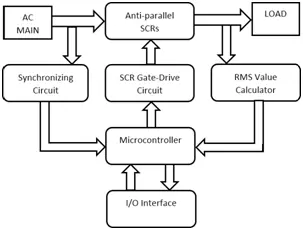
The creation of the prototype involves careful consideration across several design stages. These stages include: 1) the implementation of an anti-parallel SCR-based voltage controller, 2) the development of gate-drive circuitry for the SCRs, 3) PWM generation facilitated by a microcontroller, 4) the incorporation of phase and frequency detection, 5) calculation of the RMS value for feedback, and 6) the establishment of input-output interfacing.
The system’s functional block diagram is illustrated in Figure 1.
3. HARDWARE IMPLEMENTATION
- Voltage Control Mechanism
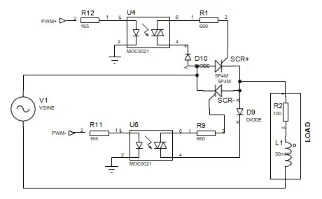
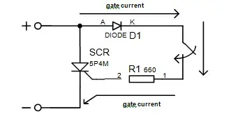
The control of AC voltage involves the utilization of a pair of anti-parallel Silicon Controlled Rectifiers (SCRs) as the switching devices. The circuit diagram for the voltage control circuit based on SCR is illustrated in Figure 2. Given the configuration, the two cathodes of the SCRs are associated with distinct nodes. As a result, it becomes imperative to isolate each gate pulse from the other. This isolation is effectively accomplished through optical coupling, facilitated by MOC3021 optocouplers, as depicted in the mechanism outlined in Figure 3 [4].
B. Synchronization
Accurate matching of phase and frequency between the PWM signals and the AC supply line is crucial. Even a minor frequency deviation can result in a gradual loss of synchronization between the PWM signals and the supply. To achieve this synchronization, a modified zero-crossing detector is employed, and the corresponding circuit diagram is illustrated in Figure 4.

The ultimate result produced by this circuit is a PWM (Pulse Width Modulation) signal that is ideally expected to exhibit a logic level 0 during the positive half cycle and a logic level 1 during the negative half cycle. Nevertheless, the introduction of resistance in the input circuit causes the signal’s mark (representing logic level 1) to commence slightly earlier than the onset of the negative half cycle and concludes slightly later (by an equivalent time duration) than the conclusion of the negative half cycle. The timing details are illustrated in Figure 5.

The time error can be determined using equation (1), which relies on the relative positions of the AC supply and the synchronization pulses.
C. PWM Generation
Controlling the SCRs requires the PWM signals to meet specific criteria: 1) The PWM signals must exhibit inversion (space preceding mark), 2) The PWM frequency must precisely match the supply frequency, 3) Access to the phase information of the supply is essential, and 4) The PWM frequencies must be twice that of the AC supply. For PWM generation, an AVR microcontroller, ATmega32, was employed [5]. While it is feasible to drive both SCRs with the same PWM signal, a slight timing mismatch can lead to unintended triggering in the subsequent half cycle.
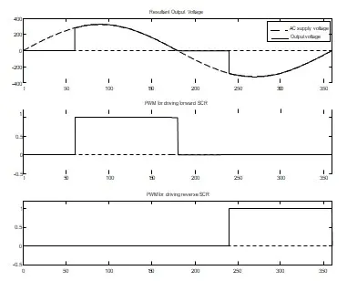
To mitigate the risk of such triggering, two PWMs operate in an interleaved manner. Consequently, during the positive half cycle, the PWM controlling the reverse SCR is set to zero, and during the negative half cycle, the PWM governing the forward SCR is also set to zero. Figure 6 illustrates the two generated PWM signals alongside the resulting output voltage, juxtaposed with the supply voltage.
D. RMS Value Calculation:
Determining the RMS value of the output poses a challenge as simply dividing the peak value by √2 is not accurate when dealing with a distorted sinusoidal wave [6]. To address this, we incorporated another microcontroller, the AVR ATmega8, for the specific purpose of calculating the RMS value of the output voltage [7]. This decision stems from the recognition that the additional computational load required for this calculation could potentially impede the time-sensitive operations of the main microcontroller. To compute the RMS value, one must sample the output voltage over a complete cycle of the supply voltage, obtaining N samples, and then apply the following equation.
Due to the limitation of the AVR microcontroller’s analogue-to-digital converter, which only facilitates the conversion of positive voltages, we leverage the symmetrical nature of the output. Consequently, the output is sampled exclusively during one half cycle. The obtained result is then transmitted to the main microcontroller to serve the feedback function.
E. Input/output Interface
To enable manual input for establishing the reference voltage value, a variable resistor has been employed. Interfacing with a 16×2 LCD module allows the display of diverse data associated with the operation. Both the reference voltage value and the resulting output voltage are presented on the LCD display. Additionally, the frequency of the supply voltage, relative to the microcontroller clock, is also showcased on the display.
4. ALGORITHM AND EXECUTION
Upon device startup, it autonomously gauges the values of Ttotal and Terror. As illustrated in Fig. 5, the ascending edge of the synchronization pulse reaches the Terror time prior to the conclusion of the positive half-cycle. Consequently, each rising edge indicates that there is Terror time remaining until the commencement of the negative clock cycle. If TPWM denotes the duration from the onset of the PWM cycle, then on each positive edge, TPWM should equate to (Ttotal/2 – Terror).
The essential pair of PWMs are not generated independently. Instead, the same PWM is routed through two distinct pins of the microcontroller, delivering them to their respective SCR drive circuits at the designated times. Following the conclusion of each PWM cycle, the pins undergo a swap. The flow chart detailing the synchronization process is depicted in Fig. 7.

The continuous update of the target output voltage value is a key aspect of the system. This target voltage is defined through a combination of manually input reference and the feedback-derived output voltage value. The voltage error (Ve or Vep) is then calculated using the formula:
\[ V_e = V_{ref} – V_{out} \ \ \ (3) \]
Rather than utilizing the error directly, a PID controller is employed. The proportional, differential, and integral components of the error are individually computed and assigned gains KP, KD, and KI, respectively. The overall error is further subjected to an overall gain, denoted as K. Consequently, the new target output voltage is determined as follows:
\[ V_{target} = K \cdot (KP \cdot P + KD \cdot D + KI \cdot I) \]
To achieve a specific value of the root mean square (RMS) output voltage (V_target), the corresponding target firing angle is determined. To facilitate this, a microcontroller stores a lookup table consisting of 64 data points. In cases where a point doesn’t precisely match the desired value, linear interpolation is applied. The target duty cycle (D) is consequently obtained from the target firing angle. Figure 8 illustrates the flowchart detailing the process of determining the target duty cycle.

5. RESULTS AND DISCUSSIONS
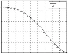
The prototype underwent testing with purely resistive loads. In Fig. 9, an input-output relationship is depicted, where the input is represented by the firing angle, and the expected output is also graphed.
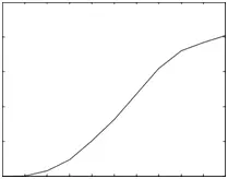
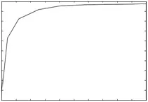
Fig. 10 illustrates the variation in output power with changing duty cycle. The relationship exhibits a non-linear nature, mirroring the correlation between voltage and duty cycle. Due to a nearly constant power loss in the operating circuit, the device’s efficiency is notably low when the power output closely aligns with this minimal power loss. However, as the load increases, the efficiency approaches unity and falls within the practical load range. Fig. 11 illustrates how efficiency changes with varying output power.
In Fig. 12, 13, and 14, the output power spectrum is presented for firing angles of 90˚, 120˚, and 150˚, respectively. The contribution of harmonics to the total output power is visibly elevated for the last two firing angles. Consequently, the recommended operational zone should involve firing angles that are less than or equal to 90˚.


CONCLUSIONS
The viability and efficacy of the proposed project are assessed through simulation studies and practical real-time implementation. The utilization of a microcontroller-based design is instrumental in enhancing its efficiency. Intelligent control based on the microcontroller enables the system to adapt effectively to various scenarios, facilitating automation responsiveness. Furthermore, the adaptability of the device can be extended to operate in high-power environments by substituting the SCR pair with high-power SCRs. Implementing filtering techniques could enhance the design by mitigating harmonic content. However, the presence of lower-order harmonics poses challenges for effective filtering.
Alternatively, a solution involves the implementation of an adaptive range selector, compelling the firing angle to be less than 90 degrees by adjusting the input voltage. This adjustment can be achieved by selecting from multiple transformers when necessary.
- What switching devices are used for high-power AC voltage control in the project?
Anti-parallel Silicon Controlled Rectifiers (SCRs) are used as the switching devices. - How are the SCR gate pulses isolated from each other?
Gate pulse isolation is accomplished using MOC3021 optocouplers. - Can the PWM and AC supply be synchronized, and how?
Yes; synchronization is achieved using a modified zero-crossing detector to match phase and frequency. - How is the PWM generated to control the SCRs?
PWM is generated by an ATmega32 microcontroller with two interleaved PWM outputs matching the supply frequency and inverted timing. - Does the system calculate RMS of the output, and which microcontroller handles it?
Yes; RMS calculation of the output is handled by a separate ATmega8 microcontroller. - How does the feedback control adjust the target output voltage?
Feedback uses PID control (KP, KD, KI) and an overall gain K to compute Vtarget from the error between Vref and Vout. - What method is used to convert target RMS voltage to firing angle or duty cycle?
A microcontroller lookup table of 64 points with linear interpolation maps Vtarget to the target firing angle and duty cycle. - What are the recommended firing angle limits to reduce harmonics?
Operating with firing angles less than or equal to 90 degrees is recommended to minimize harmonic contribution. - Can the design be scaled to higher power applications?
Yes; the device can be adapted for high-power use by substituting the SCR pair with higher-power SCRs. - What options does the article suggest to reduce harmonic effects or enforce safe firing angles?
Implementing filtering techniques or an adaptive range selector (selecting transformer taps) to keep firing angles below 90 degrees are suggested.