Summary of Intelligent Sips: Revolutionizing Dining with the SmartCup
The SmartCup Attachment monitors cup liquid levels via a base-mounted attachment that senses weight and motion, transmits RF data to a hub which converts it to Bluetooth, and an iOS app displays cup status and notifies staff. The attachment uses wireless charging, a battery, accelerometer gating, and a CC1000 RF link; the hub bridges RF to Bluetooth (HM-10). Prototype tested single-cup operation with scalable design, verified RF, charging, and sensors, and included error detection/correction in its protocol.
Parts used in the SmartCup Attachment:
- Weight Sensor (Uxcell 5kg load cell)
- Accelerometer Chip (ADXL335)
- Microcontroller (Atmel ATMega328P)
- Wireless Charging Coil (22 AWG coil)
- Transceiver (TI CC1000)
- Bluetooth Module (HM-10 / KEDSUM Bluetooth transceiver)
- Instrumentation Amplifier (INA122)
- Battery Charging IC (MAX1555)
- Voltage Regulator (LT1763)
- Polymer Lithium Ion Battery (3.7V 400mAh)
- Attachment Case (enclosure)
- Capacitors
- Resistors
- Diodes
- Inductors
- Printed Circuit Boards (PCBs)
Abstract
The SmartCup Attachment is a comprehensive system designed for restaurants to monitor the liquid levels in their customers’ cups. This system comprises the attachment affixed to the base of cups, a hub responsible for processing data from all cups and converting it into Bluetooth format, and an iOS application that seamlessly connects to the hub, presenting the data through an intuitive interface. Existing restaurant cups can be retrofitted with the attachment, which is wirelessly charged for complete convenience. The attachment and hub establish a connection using a specialized radio frequency protocol. To ensure efficient data transmission, the attachment detects cup motion, transmitting data only when the cup is stationary. Although the current design tests connectivity with a single cup, the system is easily scalable for comprehensive implementation across an entire restaurant.
1.0 : Introduction
Restaurants heavily rely on customer feedback, and enhancing customer satisfaction is crucial for improving service quality. In bustling dining establishments, wait times for drink refills can be prolonged as waitstaff struggle to attend to every table promptly. Our innovative refill cup system aims to simplify and streamline the waiter’s responsibilities by monitoring the liquid levels in each patron’s cup. When a customer’s drink is empty, the waitstaff receives instant notifications via a mobile application, reducing the time customers spend waiting for a refill. This improved efficiency leads to greater customer satisfaction, potentially increasing tips and attracting more business.
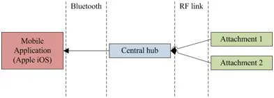
Our project introduces a multi-cup attachment system that connects to a central hub through radio frequency (RF) communication, as illustrated in Figure 1. The attachment securely fits onto the bottom of existing restaurant cups, providing water damage protection. Equipped with wireless charging capabilities and a battery life of at least six hours, the attachment ensures uninterrupted functionality during peak restaurant hours. Its primary function involves processing information from various sensors recording liquid quantity, transmitting this data via RF to the central hub. The hub performs error correction and packet parsing, formatting the information into a Bluetooth packet for communication with an iOS application. The app maintains a customer database, notifying waitstaff when a patron’s liquid level falls below a user-defined threshold for “empty.” This threshold can be manually adjusted by the user to account for variations in weight due to liquid type or cup weight. The prototype involves a single attachment connected to a hub for proof of concept, with the ultimate goal of creating a versatile product compatible with various glassware and drinking conditions.
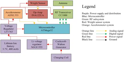
Figure 2 presents a block diagram of the attachment, highlighting power regulatory circuitry, including a charging coil and voltage regulators, to ensure a stable 3.3 V signal for sensors and the microcontroller. The microcontroller serves as a central processing unit, managing data from sensors and controlling all components, particularly the CC1000.
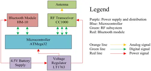
In Figure 3, the hub’s block diagram depicts minimal circuitry, encompassing power management, a microcontroller, and transmitters. The Bluetooth module facilitates data transmission to the iOS app, while the CC1000 acts as a receiver processing data from the attachment.
1.1 : Figures
2.0 : Design
2.1 : Design Alternatives
Previous endeavors in measuring liquid levels within cups have achieved moderate success. One specific attempt relies on the variation in radio-frequency identification (RFID) signal strength, which changes based on its proximity to water. However, a significant drawback of RFID technology arises when ice is present, leading to noticeably inaccurate measurements. This limitation makes the technology impractical for restaurant applications. Another project employs capacitive sensing by implementing an electrode design on the side of a custom cup. Unfortunately, this approach necessitates a substantial investment from restaurant owners, as the sensors cannot be easily affixed to existing cups in their establishments.
Our objective is to develop a product that ensures precise measurements by leveraging the movement detection capabilities of an accelerometer. Importantly, we aim to design this product to be compatible with the standard cups commonly used in most restaurants, eliminating the need for significant modifications or additional investments by restaurant owners.
2.2 : Attachment Design
Our attachment operates as a self-contained system, extracting data from multiple sensors, converting it into a transmissible format, and subsequently sending it to the hub. Comprising a weight sensor, accelerometer, microcontroller, wireless charging coil, and power regulatory circuitry, each component is individually straightforward in design. However, the overall system requires interfacing facilitated by the microcontroller.
The microcontroller integrated circuit (IC) selected for the attachment is the Atmel ATMega328p. This choice is dictated by its compatibility with the 3.3V supply necessary for the operation of all other ICs on the printed circuit board (PCB). The code for attachment operation is written in the Arduino integrated development environment (IDE) and is flashed using a four-wire in-system programming (ISP) method similar to AVRISP. The standalone microcontroller design is uncomplicated, involving only decoupling capacitors and an 8 MHz crystal. Operating the attachment at 8 MHz is essential, as the standard 16 MHz operation is not viable at 3.3V.
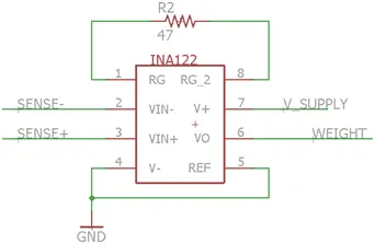
The weight sensor, a load cell affixed between the top platform and the attachment’s base, incorporates a piezoresistive segment of wire stretched between a flexible metal beam and the metal body. The sensor features a 4-pin interface (Vdd, Gnd, Sense+, and Sense-), with the analog voltage difference between the two sense signals varying linearly based on the applied force, proportional to the weight of the liquid in the cup. Unfortunately, the microcontroller cannot detect the small differential voltage from the weight sensor. To address this, we amplify the signal using the INA122 instrumentation amplifier, which offers a tunable gain according to the specifications outlined in the datasheet.
𝑉𝑜𝑢𝑡 = 𝐺(∆𝑉𝑖𝑛) 𝑤ℎ𝑒𝑟𝑒 𝐺 = 5 + 200 𝑘𝗇
𝑔
Since the weight sensor lacks an official datasheet, we had to estimate the gain by relying on information gleaned from online research paper reviews. According to these reviews, the load cell indicates a maximum differential voltage of 0.066V. This value corresponds to 3.3V when considering the gain equation of the INA122.
𝐺 = 3.3 𝑉
0.066 𝑉
= 45.45455
45.45455 = 5 + 200 𝑘𝛺
𝑅𝑔
𝑅𝑔 = 4943.82 𝛺
Upon further testing, it became evident that the initial resistor value of 4.9KΩ for our weight sensor did not yield sufficient gain. Subsequent manual testing with progressively smaller resistor values led us to settle on a value of 47Ω, nearly a thousand times smaller. Figure 4 illustrates this updated resistor value within the amplifier circuit. We suspect that our initial approximation, based on research papers, may not be applicable to this specific load cell. Access to a datasheet would likely provide more accurate values.
The accelerometer in our attachment serves as a global interrupt for data transmission, distinguishing between stationary and tilted cup positions to prevent transmitting weight data while the cup is in use. If the accelerometer detects a voltage exceeding a threshold defined in the microcontroller code, the logic rejects the weight value as faulty. We utilize the Analog Devices ADXL335, a 3.3V 3-axis analog accelerometer with 0.05G resolution to ±3G. It outputs three analog signals representing acceleration in the X, Y, and Z axes. The ADXL335’s signals can be directly connected to the microcontroller without additional interface circuitry. According to the datasheet, the zero-tilt signal is 1.55V, with a 0.07V difference for every 15 degrees of tilt. Based on manual experiments, we determined that a 15-degree tilt is appropriate for drinking. Therefore, if the last accelerometer reading exceeds 1.55 ± 0.07V, the cup has been picked up, and the weight value will not be transmitted.
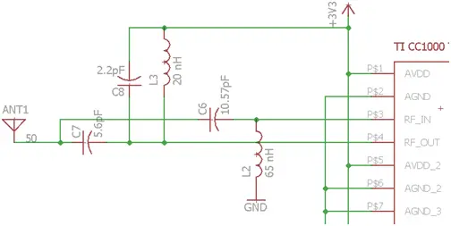
The primary circuit in our attachment design is the RF transmitter and receiver module. The RF transmitter is situated in the attachment, while the RF receiver is located in the Bluetooth hub connecting attachments to the mobile app. To simplify and standardize operations across multiple devices, we opted for a single transceiver IC connected to a microcontroller, specifically the TI CC1000. This low-power RF transceiver IC employs frequency-shift keying (FSK) modulation and a programmable digital data core. While the CC1000 datasheet offers implementation circuitry and suggested component values, it lacks guidance on designing an impedance network for the recommended monopole antenna. We employed equations from ECE 453 and ECE 457 to create the impedance matching network, ensuring compatibility between the CC1000’s impedance (88 – j26) and the antenna’s 50Ω impedance.
𝑄 = � 𝑅𝐶𝐶1000
𝑅𝑎𝑛𝑡𝑒𝑛𝑛𝑎
− 1
𝑋𝑝,𝑟𝑒𝑓 = 𝑅𝐶𝐶1000
𝑋𝑠,𝑟𝑒𝑓 = −𝑅𝑎𝑛𝑡𝑒𝑛𝑛𝑎 × 𝑄
Upon inputting the values for the parallel representation of the CC1000, the outcome is the parallel load results:
𝑄 = �95.682 − 1 = 0.9558 (2.1.6)
50
𝑋𝑝,𝑟𝑒𝑓 = 88
= 92.065 (2.1.7)
𝑋𝑠,𝑟𝑒𝑓 = −50 × 0.9558 = −47.792
The unidentified reactances of the L-network and the recognized reactances of the source and load are employed to express the lumped reactances. This formulation allows us to determine the reactances of the L-network. Given that the antenna’s input impedance is purely resistive, the series reactance aligns with the reactance of the series L-network.
𝑋𝑠,𝑟𝑒𝑓 = −47.792 = 𝑋𝑠 + 0 𝛺
𝑋𝑠 = −47.792
𝑋𝑝,𝑟𝑒𝑓
= 92.065 = 𝑋𝑝 × 323.846
𝑋𝑝 + 323.846
𝑋𝑝 = 128.633
The ultimate series and parallel reactances obtained are subsequently employed in the application of device equations to determine the final values of the capacitor and inductor.
−47.792𝑗 = 1
𝑗𝜔𝐶
128.633𝑗 = 𝑗𝜔𝐿
47.792 = 1
�2𝜋(315 × 106)�
→ 𝑪 = 𝟏𝟎. 𝟓𝟕 𝒑𝑭
128.633 = �2𝜋(315 × 106)�𝐿 → 𝑳 = 𝟔𝟓 𝒏𝑯
Figure 5 displays the final impedance network of the CC1000. The LC matching network is integrated with an LC choke designed to suppress spurious frequency noise, along with a decoupling capacitor aimed at eliminating quiescent antenna noise from the circuit to prevent transmission frequency drift.
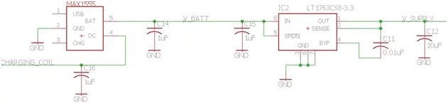
For the attachment’s power source, we employ a combination of wireless charging and a battery. A 3.7V 400mAh polymer lithium battery, chosen for its compact dimensions, powers the attachment and easily fits within the cup attachment, providing ample power for extended usage. Given the varied allowable voltage ranges of our components, we also utilize an LT1763 voltage regulator to maintain a constant 3.3V. The regulator, offering an 800mA output current, proves more than sufficient for all components. Charging of the lithium-ion battery is regulated by a MAX1555 IC, controlling voltage and current from the charging circuit to the battery. The charging circuit supplies 4.2V, stepped down to 3.5-3.9V for staged battery charging, as illustrated in Figure 6. The node V_BATT connects to the positive voltage of the lithium battery through a pushbutton switch for attachment power control.
Our attachment functions as a closed, waterproof system incorporating a wireless charging circuit. Resonant inductive coupling, utilizing an AC function generator connected to a copper wire coil, charges the internal battery. Opting for 90 KHz as the resonant frequency enhances energy efficiency significantly and minimizes power losses over distance. The choice of 100 nF capacitors simplifies practical implementation. To determine the required inductance, we begin with the formula for calculating the resonant frequency in an LC circuit, as depicted in Figure 6.
𝑓 = 1 2π√𝐿𝐶
In the provided formula, where 𝑓0 represents the resonant frequency (set at 90 KHz), 𝐿 denotes the inductance, and 𝐶 stands for the capacitance (fixed at 100 nF), rearranging the equation yields the expression for determining the inductance:
𝐿 = 1
𝐶4π2𝑓02
= 30 𝑢𝐻
We crafted the coils utilizing 22 AWG wire, employing Wheeler’s formula to obtain a preliminary estimate of the coil dimensions:
𝐼𝑛𝑑𝑢𝑐𝑡𝑎𝑛𝑐𝑒 (𝑢𝐻) = 1
6𝑟1+9𝐿+10(𝑟2−𝑟1)
Where N represents the number of turns, r1 denotes the radius of the inner coil, r2 stands for the radius of the outer coil, and L signifies the length of the wire within the coil. Our design entails a coil with a two-inch diameter, half an inch thickness, and 22 turns.
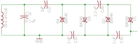
Connected to the charging coil on the attachment is a Cockcroft-Walton voltage generator, which amplifies the high-frequency charging coil voltage into a DC high-voltage output. Initially, our intention was to convert the 1.25V AC voltage from the charging coil into a 5V DC voltage, sufficient for the MAX1555 to regulate the charging of our lithium battery. The equation governing the voltage gain in the multiplier we employed was:
𝑉0 = 2𝑁𝑉𝑃 = 2 × 2 × 1.25 = 5 𝑉
In Figure 7, the configuration of the Cockcroft-Walton voltage generator is outlined. Each stage incorporates two diodes and a capacitor. The diodes serve to rectify the voltage, permitting charging only during the rising or falling edges of the input AC sine wave received from the charging coil. Through the accumulation of charge, the capacitors amplify the voltage at each node by a factor of two. By sequentially connecting two sections, we can elevate the voltage to the 5 V level as described in Equation .
The operational sequence of the entire attachment device is outlined in the step-by-step walkthrough below. Figure 8 provides an overview of the CC1000’s transmit and receive modes in response to sensor conditions.
1. Upon device power-on, the LT1763 and MAX1555 ICs maintain a 3.3V supply from the 3.7V lithium battery. This action initializes the microcontroller, activates the RF transceiver, and powers all other devices on the board.
2. The microcontroller proceeds to configure the transceiver into specific operating modes. Utilizing the 3-wire interface (PCLK, PDATA, and PALE), the microcontroller programs baud rate and frequency spectrum parameters through a series of memory-mapped register accesses. Two diagnostic tests [1] are conducted to validate IC operation. The process concludes with an interrupt request to transition the system into a receive state.
3. Following the completion of the transceiver setup, the microcontroller continuously samples values from the accelerometer and the weight sensor. During the initial sample, it checks if the accelerometer reading falls below the thresholds of 1.55 ± 0.07V. At this point, it encodes the weight and additional device information into a three-byte RF packet.
4. The microcontroller triggers an interrupt signal to switch the transceiver to transmit mode. Configuration information, specifying frequency details and data encoding, is sent to the transceiver. The data is transmitted, and the microcontroller waits for the Received Signal Strength Indicator (RSSI) pin to go high, indicating the completion of data transfer.
5. Steps 3 and 4 are repeated every 10 seconds within an internal microcontroller loop, ensuring the transmission of one data packet every 10 seconds. If, at any point, the accelerometer reading exceeds the thresholds of 1.55 ± 0.07V, all data from the weight sensor is discarded. The microcontroller then waits for a reading within the threshold. Once a reading indicates that the cup has been placed back down, the weight sensor is sampled, and data is transmitted to the transceiver following the steps outlined in 3 and 4. The accelerometer, operating as an asynchronous interrupt within the default 10-second transmit regime, holds the highest priority in deciding whether data will be sent across the system or not.
2.3 : Hub Design
The hub serves as the interface between the attachment’s RF information and the Bluetooth antenna of the iOS application. Consequently, the hub comprises fewer components compared to the attachment. Its components include a microcontroller, RF receiver, Bluetooth module, and power regulation circuitry. Due to the complexities associated with the design of PCBs and circuits related to Bluetooth technology, we found it challenging to design and test a complete Bluetooth package. Adhering to Apple’s restrictions on Bluetooth specifications and model compatibility, we opted for an Apple-approved Bluetooth 4.0 module, specifically the HM-10 Bluetooth 4.0 low-energy module. This choice aligns with Apple’s authorization, ensuring full compatibility with iOS software.
The power regulation circuitry for the hub is simpler than that of the attachment. As the hub is designed for long-term use, sporadic data handling, and is not at risk of spillage or damage like the attachment, there is no need to incorporate wireless charging. Consequently, the power circuitry consists of three AA batteries supplying 4.5V to an LT1763 regulator, which in turn provides 3.3V to the other components on the hub’s PCB. The hub’s microcontroller performs the task of converting the RF data packet from the attachment into a packet format that aligns with Apple’s Bluetooth specifications. The circuitry for the microcontroller mirrors that of the attachment, and the code includes error correction and detection for the transmitter’s data. The following procedure outlines the operational steps for the hub:
1. Powering on the hub activates the microcontroller, transceiver, and Bluetooth module. The microcontroller remains in an idle state until the Bluetooth module completes its startup, as it takes longer than the microcontroller.
2. The microcontroller configures the transceiver into specific operating modes. Using the 3-wire interface (PCLK, PDATA, and PALE), the microcontroller programs baud rate and frequency spectrum parameters through memory-mapped register accesses. Two diagnostic tests [1] are conducted to validate IC operation. The process concludes with an interrupt request to transition the system into a receive state. The hub’s transceiver never transmits data to the attachment, so the transmit mode is never enabled.
3. Received data undergoes processing for error detection when it reaches the microcontroller. After correcting any errors, it is stored in a message translation buffer. During each cycle, a message is removed from the buffer.
4. The data from the buffer is encoded with a transaction address and advertising channel ID computed based on the number of available attachment devices and the central device running the mobile application. Following this encoding, it is packaged as a Bluetooth payload and transmitted to the Bluetooth module via a serial interface.
5. The Bluetooth module reads data from the serial interface and transmits the complete packet to the mobile application.
2.4 : Mobile Application Design
The concluding segment of our project involves the mobile app, utilized to visually monitor liquid levels in the attachments through a three-color system integrated into the graphical user interface (GUI). The app depicts an empty cup for each attachment device, featuring an indicator rectangle within the cup. This rectangle dynamically changes color (green to yellow to red) and diminishes in size, reflecting the liquid level detected by the attachment. The phone serves as the central device consistently seeking packets sent from the peripheral (hub). Figure 9 provides a basic illustration of how our hub (peripheral device) transmits advertising packets to the phone (central device) for discovery.
Representatively, the phone is depicted by a CBCentralManager object, while the hub is a CBPeripheral object. When transmitting data packets, the peripheral dispatches CBService objects containing multiple CBCharacteristics such as weight and cup ID. The detailed workflow of how the phone reads packets from the hub is outlined step-by-step:
1. Discover the hub
a. Invoke the scanForPeripheralsWithServices:options: method from the CBCentralManager class.
2. Connect to the hub after discovery
a. Request connection to the peripheral by calling the connectPeripheral:options: method of the CBCentralManager class.
b. Implement each discovered service as a CBService object when specific data (services) are found.
3. Discover the specifics of the data packet
a. Each service sent by the hub will encompass several characteristics defining the data within a data packet.
4. Retrieving the data
a. Upon identifying the weight characteristic of the service, employ the readValueForCharacteristic method of the CBPeripheral class.
5. Display the data on the UI.
2.5 : RF Communication Protocol
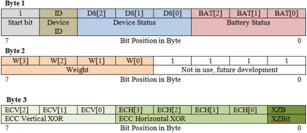
The communication between the attachment and hub relies on a proprietary protocol resembling that of serial communication. This protocol comprises a preamble, calibration details, a 3-byte data packet, and an end-of-message byte. The preamble and calibration information are configured based on the CC1000 datasheet, while the end-of-message byte is consistently set as xAA. Figure 10 provides a breakdown of the bitfields within the data packet.
Byte 3 encompasses supplementary details pertaining to error detection and correction in the transmitted signal. While the ideal scenario involves error-free data transmission, factors such as noise and distance can influence the performance and reliability of the data received from the microcontroller. This byte incorporates check bits against which the computed data is compared to ascertain whether an error has occurred. The task is to generate an ECV, ECH, or XZB bit value that satisfies the following equations.
The identical algorithm is utilized within the hub to produce a new collection of internally encoded ECV, ECH, and XZB values represented as Generated Byte 3 (GB3). Assuming there are no errors, GB3 should align with B3, allowing the data to undergo Bluetooth encoding. In the event that GB3 does not correspond to B3, two XOR equations are generated, resulting in a parity mismatch. This mismatch signals the specific bit that requires inversion for error correction. As this algorithm exclusively identifies and rectifies single-bit errors, the packet is considered defective and rejected if multiple bit errors are detected.
2.6 : Figures

3.0 : Verification and Results
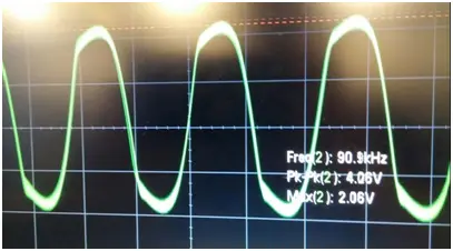
The system verification process comprised four key testing stages. Initially, post-PCB-assembly testing was conducted, wherein each component underwent probing on the PCB. Voltages and currents were examined using a multimeter or oscilloscope. This initial stage revealed issues in the weight sensor, specifically in the theoretical resistor value, which failed to generate a significant voltage gain from the INA122 amplifier. The first stage confirmed the functionality of microcontroller voltages, RF transceiver voltages, wireless charging and power circuitry, and the weight sensor. Figure 11 illustrates the oscilloscope verification of the charging coil’s requirements.
The second verification stage focused on programming aspects. The microcontroller’s programming code was utilized to read and process values from sensors and peripherals for accuracy determination. Components like the RF transceiver underwent verification through specific byte sequences or data patterns sent and received via a three-wire serial bus. This stage, which included writing testing code for each peripheral, took considerable time. Verification of the iOS app’s host processes and services through the XCode IDE and console monitor was also part of this stage, with the design and verification of the app being less time-consuming than that of hardware devices.
The third verification stage involved a comprehensive system integration test, where all components collaborated on the attachment and hub. Delays were introduced into the final microcontroller code to allow sufficient time for reaction and settling. Serial monitor commands were employed to display confirmation at each major step of the attachment and hub operation. Several issues, such as current draw and RF interference of the RF transmitter and the instrumentation amplifier, surfaced during this stage, unlike the second stage where individual component operation showed no conflicts. These problems were addressed by incorporating calibration code to transition the CC1000 into a low-power high-impedance state when making measurements from the weight sensor and accelerometer.
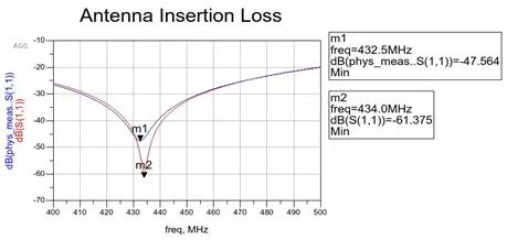
The concluding phase of the testing process focused on instrumentation analysis to assess the reliability of the RF and Bluetooth systems. Utilizing a network analyzer, spectrum analyzer, and antenna array network, we characterized the RF parameters of both the attachment and hub, including reception gain, insertion loss, and coupling factor. The network analyzer provided numerical data for the frequency performance of the monopole antenna, aligning with simulations. In Figure 12, the red curve S(1,1) represents the simulated impedance network’s insertion loss response, while the blue phys_meas(1,1) curve depicts normalized measurements from the network analyzer. Clearly, the minimum frequency falls within R&V tolerances of the central RF frequency, and the decibel reception level is below the 30 dB requirement, confirming the successful operation of the antenna and impedance network on the PCB.
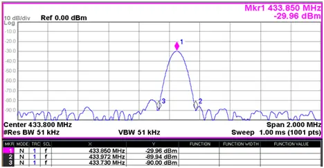
Subsequent RF testing involved tolerance analysis, as outlined in our design review. Given that distance significantly influenced our choice of RF protocol for communication between the attachment and hub, it was imperative to ensure the attachment could transmit an RF signal with a high power level. As illustrated in Figure 13, reception at 1.5 feet demonstrated that the transmitter broadcasted a signal within our requirements, with a 200 KHz bandwidth, well below our specified 10 MHz bandwidth.
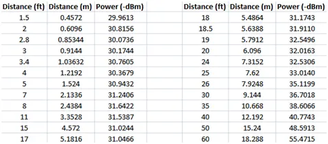
Additionally, long-range testing was conducted, not explicitly detailed here, where the RF transmitter, located 150 feet away in a separate room, successfully transmitted a recognizable signal of -78.8 dBm. This achievement occurred despite the extended distance and the presence of attenuative materials like classroom walls and other equipment. Figure 14 presents data from our tolerance analysis across various distances.
3.1 : Figures
4.0: Parts and Cost Analysis
Table 1: Labor Analysis
| Name | Hourly Rate | Hours Working | Salary (Hourly Rate x 2.5 x hours to complete) | |
| Harington Lee | $30 | 230 | $17,250 | |
| Arjun Sharma | $30 | 230 | $17,250 | |
| Chirag Patil | $30 | 230 | $17,250 | |
| Total | 690 | $51,750 |
Table 2: Component Costs
| Part Name | Quantity | Cost |
| Weight Sensor (Uxcell 5kg) | 2 | $15 |
| Accelerometer Chip (ADXL335) | 2 | $20 |
| Microcontroller (ATmega328P-PU) | 3 | $10 |
| Charging Coil (22 AWG) | 2 | $5 |
| Transceiver (CC1000) | 3 | $25 |
| Attachment Case | 1 | $3 |
| Polymer Lithium Ion Battery (400mAh) | 2 | $14 |
| KEDSUM Bluetooth Transceiver | 1 | $10 |
| Amplifier (INA122UA) | 2 | $0 (Samples) |
| Battery Charging Adapter (MAX1555) | 2 | $4 |
| Voltage Regulator (LT1763) | 3 | $0 (Samples) |
| Capacitors | 28 | $1.70 |
| Resistors | 25 | $1.2 |
| Diodes | 4 | $0.10 |
| Inductors | 8 | $1.10 |
| PCBs | 2 | $66.00 |
| Total | $176.10 |
Table 3: Total Cost
| Labor Cost | Parts Cost | Total Cost |
| $51,750 | $176.10 | $51,926.10 |
- How does the attachment detect when to transmit weight data?
The accelerometer (ADXL335) determines if the cup is stationary by checking if readings are within 1.55 ± 0.07V; weight data is transmitted only when within that threshold. - Can existing restaurant cups be used with this system?
Yes; the attachment is designed to retrofit existing restaurant cups by fitting onto their bottoms. - How is the attachment powered and charged?
The attachment uses a 3.7V 400mAh polymer lithium battery and is wirelessly charged via a resonant inductive coupling charging coil and a Cockcroft-Walton voltage multiplier feeding the MAX1555 charging IC. - What wireless protocol links the attachment to the hub?
The attachment uses a proprietary RF protocol over a TI CC1000 transceiver employing frequency-shift keying (FSK) to communicate with the hub. - How does the hub communicate data to the iOS app?
The hub converts RF packets from attachments into Bluetooth packets and sends them via an Apple-approved Bluetooth 4.0 module (HM-10) to the iOS app. - What components amplify the load cell signal for the microcontroller?
The small differential output from the load cell is amplified by an INA122 instrumentation amplifier before being read by the microcontroller. - Does the system perform error detection on RF packets?
Yes; Byte 3 in the 3-byte packet contains check bits used by the hub to detect and correct single-bit errors before Bluetooth encoding. - How often does the attachment transmit data when stationary?
The microcontroller sends one data packet every 10 seconds while the cup remains within the accelerometer thresholds. - Is the RF link designed to work at restaurant distances?
Yes; testing showed reliable reception at 1.5 feet and recognizable signals at 150 feet (−78.8 dBm) through walls and attenuating materials. - What role does the microcontroller have in the attachment?
The ATMega328P samples sensors, applies accelerometer gating, encodes weight and device info into RF packets, and controls the CC1000 transceiver.