Summary of How to use inbuilt EEPROM of PIC18F4550 Microcontroller
This project demonstrates using the PIC18F4550 microcontroller's built-in EEPROM for data storage via serial communication. Data received from a PC is stored in the internal EEPROM and can be retrieved and sent back through the USART module. The system operates asynchronously at 9600 baud, utilizing specific control registers to manage transmission and reception while handling EEPROM write sequences with proper safety protocols.
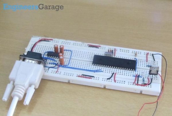
Parts used in the PIC18F4550 EEPROM Project:
- PIC18F4550 Microcontroller
- Built-in EEPROM Memory
- USART Module (EUSART)
- TXSTA Register
- RCSTA Register
- SPBRG Register
- PC (Personal Computer) for Serial Communication
The EEPROM (ELECTRICALLY ERASABLE PROGRAMMABLE READ ONLY MEMORY) is a very useful memory which can be used for storing data. The data storing and retrieving from any EEPROM memory is very simple compared to other kind of memories. As the name suggest the memory is electrically programmable and hence the data will be sustained in the memory until it is electrically erased or reprogrammed.
There are lots of EEPROM chips available most of them are easy to interface with a microcontroller. It would be even better if the microcontroller itself has a built-in EEPROM. The microcontroller used in this project is PIC18F4550 and it also has an inbuilt EEPROM memory other than the flash memory. The data can be easily stored into or retrieve using simple codes.
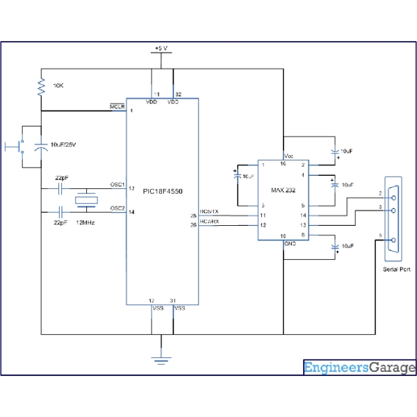
 The project mainly has two parts, a serial communication part and EEPROM accessing part. The data which should be written into the EEPROM is received from the serial port. The internal hardware module USART is used for this purpose. The data which is read from the EEPROM is also send back to the serial port using the same hardware module.
Hence two internal modules of the PIC18F4550 are used in this project namely EEPROM and USART. These hardware modules can be accessed and controller by simply writing into or reading from their corresponding registers.
The important control registers associated with the USART and their details are given below:
TXSTA: TRANSMIT STATUS AND CONTROL REGISTER
This register has the bits which controls the serial transmission features like enable or disable the transmission, whether it should be synchronous asynchronous etc.
For a simple asynchronous serial transmission only two bits are significant, which are TXEN and SYNC
TXEN is the transmission enable/disable bit and SYNC sets the synchronous/asynchronous mode.
TXEN: Transmit Enable
1 = Transmit enabled
0 = Transmit disabled
SYNC: EUSART Mode Select bit
1 = Synchronous mode
0 = Asynchronous mode
RCSTA: RECEIVE STATUS AND CONTROL REGISTER
This register has the bits which controls the serial reception features like enable/disable the serial port, reception should be 8 bit or 9 bit, whether it should be synchronous asynchronous, enable/disable continuous reception etc.
For a simple asynchronous serial reception the significant bits are SPEN, RX9 and CREN.
SPEN: Serial Port Enable bit
1 = Serial port enabled
0 = Serial port disabled
RX9: 9-Bit Receive Enable bit
1 = Selects 9-bit reception
0 = Selects 8-bit reception
CREN: Continuous Receive Enable bit
1 = Enables receiver
0 = Disables receiver
SPBRG: EUSART BAUD RATE GENERATOR REGISTER
This is a 16 bit register into which the value corresponding to the required baud-rate can be written into. The value according to a particular baud-rate can be calculated from the CPU clock frequency according to the following equation;
SPBRG = ((FOSC/Desired Baud Rate)/64) – 1
Where; FOSC is the CPU clock frequency
 SPBRG = spbrg_value; // Fill the SPBRG register to set the Baud Rate
- How is the CPU clock frequency configured?
The OSCCON register is set to 0x72 to establish a 8 MHz CPU frequency. - What formula calculates the SPBRG value?
The formula is SPBRG = ((FOSC/Desired Baud Rate)/64) – 1. - Which bits control asynchronous mode in TXSTA?
The SYNC bit must be set to 0 for asynchronous mode, while TXEN enables transmission. - How does the code enable continuous reception?
The CREN bit in the RCSTA register is set to 1 to enable the receiver. - What triggers the full EEPROM read sequence?
Receiving the data byte 0x1A initiates reading all data from address 0 to 255. - Why are interrupts disabled during EEPROM writing?
Interrupts are disabled by setting INTCONbits.GIE to 0 before writing to EECON2. - What values must be written to EECON2 sequentially?
The values 0x55 followed immediately by 0xAA must be written to EECON2. - How is the write operation finalized in EECON1?
The WR bit (0x02) is set in EECON1 to start the write cycle. - What happens after the EEPROM read loop completes?
The program enters an infinite loop (while 1) after transmitting all stored data. - Which port is configured as output for LEDs?
PORTB is set as output with TRISB initialized to 0x00.