Summary of FLIR BOSON CAMERA FRAME GRABBER USING FPGA
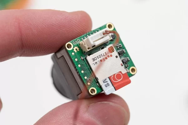
This project describes a compact PCB designed to attach to the FLIR Boson Thermal Camera, enabling configuration and image capture to an SD card. Built around a Lattice ECP5 FPGA with 64Mbit RAM and 8Mbit FLASH, it utilizes an internal RISCV CPU for tasks like UART and FatFS while dedicated hardware manages video streams via a 4-bit SD protocol. The system uses Wishbone buses connected by `wb_intercon` and supports HyperRAM DDR modules, achieving approximately 3 FPS capture rates on Boson 640 cores.
Parts used in FLIR Boson Camera Frame Grabber:
- FLIR Boson Thermal Camera
- Lattice ECP5 FPGA
- 64Mbit RAM (HyperRAM DDR modules)
- 8Mbit FLASH
- RISCV CPU (internal to FPGA)
- SD Card
- Wishbone bus components
- wb_intercon module
- PLL (Phase-Locked Loop) of the ECP5 FPGA
DESCRIPTION
The PCB facilitates configuration of the camera along with capturing data to an SD card.
This project is mostly an exercise in project-based learning. Instead of researching and reading about FPGAs, I want to create a project actually using them. Of course, this means that I’ll likely get things wrong, but that’s just part of the learning experience.
A huge shoutout to Group Gets, without their support this project would not have made it this far! They are a FLIR Boson Distributor, check out their range here: https://store.groupgets.com/collections/flir-boson-accessories
This project is a miniature FPGA based PCB to capture and save images from a camera stream. The FPGA used in the lattice ECP5, the board has 64Mbit of RAM and 8Mbit of FLASH. It runs a RISCV CPU internally to handle the processor centric tasks (UART, state machine, FatFS), but has dedicated hardware to handle the video stream and communicate to the SD card using 4bit SD protocol.
The modules inside the FPGA follow the following bus diagram. They all make use of a common wishbone buses.
All bus connections are created by this project: https://github.com/olofk/wb_intercon. wb_intercon automates the creation of muxes and arbiters required to connect various wishbone components including multiple masters.
After working on updating the verilog module used in my camera to support the HyperRAM using DDR modules and the PLL of the ECP5 FPGA I’m using.
The change increased the performance by 4x. This enables us to capture the datarate from the Boson 640 cores.
Here is a photo of the water tank ~80% full.
For reference here is the same tank using the Boson 320 core.
There are still many performance improvements I have on a list to work on.
But the major functionality of the device is working. We can capture Images at about 3 FPS. Here is the layout of the internal modules in the FPGA
Read more: FLIR BOSON CAMERA FRAME GRABBER USING FPGA
-
What is the primary function of this PCB?
The PCB facilitates configuration of the FLIR Boson camera and captures data to an SD card. -
Which FPGA chip is used in this project?
The project uses the Lattice ECP5 FPGA. -
How much RAM and FLASH does the board contain?
The board has 64Mbit of RAM and 8Mbit of FLASH. -
Can the device run at 3 FPS with the Boson 640 core?
Yes, the major functionality allows capturing images at about 3 FPS using the Boson 640 cores. -
What bus architecture connects the internal modules?
All modules make use of a common wishbone bus. -
How was the performance increased by 4x?
Performance increased by updating the Verilog module to support HyperRAM using DDR modules and the PLL of the ECP5 FPGA. -
What tool automates the creation of muxes and arbiters?
The project uses wb_intercon to automate the creation of muxes and arbiters required to connect various wishbone components.