Summary of Crafting a Microcontroller-Based Temperature Monitoring System
This thesis describes designing a portable, low-power temperature data logger using an 8051-family microcontroller (AT89C51). It acquires multi-channel temperature signals via LM35 sensors through an ADC0808/0809, timestamps and stores readings in external EEPROM (AT28C64), and displays data on an HD44780 LCD. A 4×4 keypad enables user interaction. The system emphasizes real-time logging, sequential EEPROM storage, accuracy validation against a clinical thermometer, and thorough hardware/software integration and testing across varied conditions.
Parts used in the Data Logger Project:
- LM35 Temperature Sensor
- ADC 0808/0809 Analog-to-Digital Converter
- AT89C51 Microcontroller
- 4×4 Keypad Matrix
- HD44780 Liquid Crystal Display (LCD)
- AT28C64 External EEPROM
- Clock source (for ADC and microcontroller)
- PCB and associated passive components (resistors, capacitors)
Abstract
As technological advancements progress, processes become increasingly intricate, demanding a corresponding expansion in the parameters necessary for efficient analysis. Data acquisition, the systematic gathering of information regarding systems or procedures, involves automated collection from both analog and digital measurement sources such as sensors and testing devices.
In earlier eras devoid of widespread computing capabilities, data recording primarily relied on manual techniques or strip-chart recorders. However, the emergence of microcontrollers has heralded a new era in data acquisition, enabling real-time gathering, analysis, logging, and visualization. Consequently, there is a growing need for improved, efficient, and modern data loggers to meet evolving demands.
A data logger functions as an electronic device capable of recording digital or analog measurements over extended durations. Typically composed of a sensor, microcontroller, and data storage component, data loggers are equipped with onboard memory sufficient for storing data collected over extended periods. This memory may utilize various technologies such as flash memory, EEPROM, or battery-backed Static Random Access Memory (SRAM). Additionally, data loggers incorporate real-time clocks to timestamp acquisitions.
This thesis centers on the development of a data logger tailored for a specific application within the renowned 8051 microcontroller family. Engineered to monitor temperature using dedicated sensors, the system stores acquired data in memory, such as EEPROM, for subsequent analysis. Rigorous testing validates consistent and accurate data acquisition, with sequential storage in memory confirmed through an LCD display.
Prioritizing portability and low power consumption for battery-operated scenarios, the designed system undergoes comprehensive testing across a range of conditions, including varying temperatures and extended timeframes. These assessments affirm the system’s dependable performance across diverse environmental settings.
Introduction
Logging, encompassing the processes of data collection, analysis, and storage for future reference, serves as a method to document events during testing or measurements utilizing a system or product. While the human brain, a marvel of nature’s design, serves as an exceptional data logging mechanism, there are situations where faster information collection and heightened accuracy are imperative. In such cases, data loggers prove invaluable.
A data logger, as defined, is a device utilized for the storage and retrieval of data. Additionally, data logging entails the control of how sensors collect and analyze data. Widely employed in scientific experiments and monitoring systems, data loggers autonomously record instrument readings from various points within a plant or system. The specific information recorded is customizable by the user.
One of their primary advantages is their ability to function independently of a computer, offering flexibility and convenience. Furthermore, data loggers are available in a myriad of configurations, ranging from simple single-channel fixed-function loggers to sophisticated programmable devices capable of managing numerous inputs simultaneously.
Temperature, an inherently variable parameter, fluctuates in response to a myriad of stimuli from the surrounding environment. Its measurement can be accomplished through a diverse range of sensors, each of which gauges temperature by detecting alterations in physical characteristics. However, it’s crucial to exercise caution when measuring temperature to ensure alignment between the measuring instrument (e.g., thermometer, thermocouple) and the material being measured. Under certain conditions, the heat emanating from the measuring instrument can introduce a temperature gradient, resulting in a discrepancy between the measured temperature and the actual temperature of the system. In such instances, the measured temperature not only varies with the system’s temperature but also with the heat transfer properties inherent to the system [3].
The aim of this project is to employ data logging for temperature monitoring. To fulfill this objective, a cost-effective, adaptable, and portable data logger is devised. This data logger, centered around a microcontroller, is crafted to measure temperatures across multiple input channels of an Analog-to-Digital Converter (ADC). It functions by gathering data from temperature sensors and saving the findings onto external non-volatile Electrically Erasable Programmable Read-Only Memory (EEPROM) for subsequent analysis. Additionally, an integrated Liquid Crystal Display (LCD) is utilized to provide real-time visualization of data acquired from diverse sensors.
In this study, temperatures measured across three channels are periodically compared with the standard temperature recorded by a clinical thermometer. The accuracy of each channel is assessed based on these comparisons, ultimately identifying the most precise among them.
Literature Review
2.1 Introduction to data loggers
The data logger serves as an indispensable instrument for gathering and examining experimental data. It possesses the capability to provide real-time analysis, utilizing sensors and probes capable of detecting parameters that extend beyond the typical range accessible through conventional equipment [4].
Variations among different data loggers stem from the methods employed for recording and storing data.
2.1.1 Definition of Data Loggers
A data logger is an electronic apparatus designed to automatically capture, scan, and retrieve data swiftly and efficiently during tests or measurements conducted at various locations within a facility [4]. The specific type of information recorded by the data logger is customizable, based on user preferences. Whether it’s temperature, relative humidity, light intensity, voltage, pressure, or shock, the data logger can automatically measure electrical outputs from various transducers and log the corresponding values.
Operating in conjunction with sensors, the data logger transforms physical phenomena and stimuli into electronic signals, typically in the form of voltage or current. These electronic signals are subsequently converted into binary data, facilitating easy analysis by software. The recorded binary data is then stored in memory, ready for post-process analysis.
2.1.2 Characteristics of Data Loggers:
2.1.3 Operation of data logger:
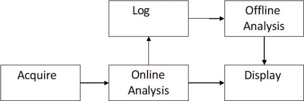
Acquire: This stage involves your sensor and data logger hardware, along with the conversion of physical phenomena into digital signals.
– Long-term storage capabilities for storing data over extended periods.
– Data logging software that facilitates data acquisition, analysis, and presentation.
2. They have the capability to function autonomously, independent of a computer, and come in diverse shapes and sizes.
3. The spectrum of data loggers spans from basic single-channel inputs to multifaceted multichannel devices.
2.1.5 Applications of Data Loggers:
Data loggers find application in various scenarios, including:
1. Unattended recording at weather stations, capturing parameters such as temperature, wind speed/direction, solar radiation, and relative humidity.
2. Hydrographic recording for water flow, pH levels, conductivity, water level, and depth.
3. Monitoring soil moisture levels through recording.
4. Tracking gas pressure and tank levels.
5. Transportation monitoring, troubleshooting, educational science, quality studies, field studies, and general research.
6. Facilitating remote data collection and alerting for abnormal parameters by integrating data loggers with modems and cellular phones.
System Design and Implementation
In crafting and refining the system, the methodology adopted encompasses both software and hardware implementation. The actual execution of the system proceeds through the subsequent stages:
System Definition: The comprehensive scope of system hardware encompasses elements such as microcontrollers and their interfaces with displays, ADCs, memory modules, keypads, and more.
3.1 Hardware Implementation
3.1.1 Component selection and description
The temperature measurement process employing a microcontroller-based data logger incorporates the following elements:
1. Temperature Sensor (LM35)
2. Analog to Digital Converter (ADC 0808)
3. Microcontroller (AT89C51)
4. Keypad Matrix (4×4 matrix)
5. Liquid Crystal Display (HD44780)
6. External Memory (AT28C64)
1.) Temperature Sensor
Selection of Suitable Transducer:
Selecting the appropriate sensor is crucial for temperature measurement [7].
Various types of sensors are employed across different fields, including Thermocouples, Resistive Temperature Devices (RTDs), thermistors, and bimetallic devices. When choosing a sensor, several factors are considered, such as inherent accuracy, durability, operational range, susceptibility to external noise, ease of maintenance and installation, delicacy during handling and installation, calibration simplicity, and the environmental conditions it will encounter.
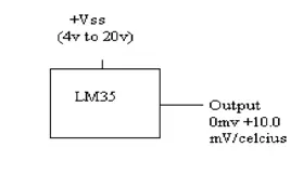
The LM35 temperature sensor is chosen for this application due to the following features:
Features of LM35:
1. Calibrated directly in degrees Celsius (Centigrade).
2. Features a linear scale with a scale factor of 10.0 mV per degree Celsius.
3. Ensures accuracy within 0.5°C (at +25°C).
4. Rated for operation across the full temperature range of -55°C to +150°C.
5. Ideal for remote applications.
6. Offers cost-effectiveness owing to wafer-level trimming.
7. Operates within a wide voltage range of 4 to 30 volts.
8. Exhibits low current drain of less than 60 µA.
9. Demonstrates low self-heating, with a mere 0.08°C in still air.
10. Features minimal nonlinearity, typically within ±1⁄4°C.
The LM35 series comprises precision integrated-circuit temperature sensors, featuring an output voltage linearly proportional to Celsius temperature. This design advantageously eliminates the need for subtracting a constant voltage to achieve convenient Centigrade scaling, unlike linear temperature sensors calibrated in Kelvin. The LM35 requires no external calibration or trimming to achieve typical accuracies of ±1⁄4°C at room temperature and ±3⁄4°C across the full -55 to +150°C temperature range. Its low output impedance, linear output, and inherent precision calibration facilitate easy interfacing with readout or control circuitry. Additionally, it can be utilized with single power supplies or with both positive and negative supplies.
2.) Analog to Digital Converter (ADC)
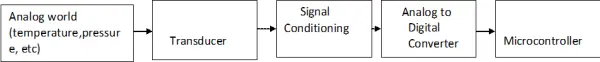
In the realm of the physical world, various parameters like temperature, pressure, humidity, and velocity are conveyed through analog signals. These signals, representing physical quantities, are translated into electrical signals. To enable a microcontroller to interpret these signals, an analog-to-digital converter (ADC) is necessary. Essentially, an ADC is an electronic circuit designed to convert continuous analog signals into discrete digital numbers. Widely employed for data acquisition purposes, analog-to-digital converters play a pivotal role in facilitating the translation of analog signals into digital formats.
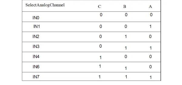
The ADC 0804 chip is widely utilized, but for this project, we’ve opted for the ADC 0809 analog-to-digital converter. Unlike the ADC 0804, which has only one analog input, the ADC 0809 provides eight analog inputs. This feature enables the monitoring of up to eight different transducers using a single chip. The eight analog input channels are multiplexed and can be selected as needed.
In the ADC 0808/0809 models, the reference voltage is determined by Vref(+) and Vref(-). Setting Vref(-) to Gnd and Vref(+) to 5V establishes a step size of 5V/256, resulting in approximately 19.53mV. Therefore, to achieve a step size of 10mV, we must adjust Vref(+) to 2.56V and Vref(-) to Gnd.

The process of transferring data from the analog input of the ADC 0808/0809 to the microcontroller involves the following steps [7]:
1. Begin by selecting an analog channel and providing the appropriate bits to the A, B, and C addresses. Then, activate the ALE (address latch enable) pin with an L-to-H pulse to lock in the address.
2. Trigger the start of conversion (SC) by generating an H-to-L pulse, initiating the conversion process.
3. Monitor the end of conversion (EOC) to determine if the conversion is complete. A transition from H-to-L indicates that the data has been converted and is ready for retrieval.
4. Activate the output enable (OE) to extract data from the ADC chip. An H-to-L pulse applied to the OE pin facilitates the extraction of digital data from the chip.
It’s important to note that the ADC 0808/0809 lacks a self-clocking mechanism, requiring an external source to provide the clock signal to the CLK pin.
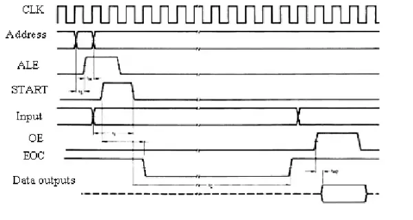
Each approximation cycle of the ADC0808/ADC0809 comprises 8 clock periods, even when there is no ongoing conversion [9]. Although a start pulse may be initiated at any point during this cycle, the actual conversion will commence only when the converter internally resets to the beginning of the subsequent 8-clock period sequence. While the start pin remains in a high state, no conversion initiates. However, once the start pin transitions to a low state, the conversion will commence within 8 clock periods. The EOC (end of conversion) output is triggered by the rising edge of the start pulse. Like other aspects of operation, it is synchronized with the 8-clock period cycle, causing it to transition to a low state within 8 clock periods of the rising edge of the start pulse. It’s worth noting that the EOC may transition low before the internal conversion starts; however, this isn’t critical, as the control logic primarily seeks the positive transition of EOC, which signifies the completion of the conversion process. Once EOC transitions high, it indicates to the interface logic that the conversion result data is ready for retrieval. Subsequently, the output enable (OE) is activated to enable data readout.
3.) Microcontroller chip
1. The primary consideration when selecting a microcontroller is its ability to efficiently and cost-effectively address the task at hand. When evaluating the requirements of a project based on a microcontroller, the suitability of an 8-bit, 16-bit, or 32-bit microcontroller is assessed to determine which can best fulfill the computing needs of the task. Additional factors in this category include:
(a) Speed – What is the maximum speed supported by the microcontroller?
(b) Packaging – Does it come in a 40-pin DIP (dual inline package), QFP (quad flat package), or another packaging format? This is crucial concerning space, assembly, and prototyping of the end product.
(c) Power consumption – Particularly crucial for battery-powered devices.
(d) Number of I/O pins and onboard timers.
(e) Ease of upgrading to higher-performance or lower-consumption versions.
(f) Cost per unit – Significant in determining the final product cost in which the microcontroller is utilized.
2. The second criterion in microcontroller selection is the ease of product development around it. Key considerations include the availability of an assembler, debugger, and a compiler that optimizes code efficiency, as well as the provision of technical support.
3. The third criterion is the microcontroller’s availability in required quantities both presently and in the future. Currently, among leading 8-bit microcontrollers, the 8051 family boasts the largest number of diverse suppliers. When referring to suppliers, this indicates producers apart from the microcontroller’s originator. In the case of the 8051, while initially introduced by Intel, several other companies also manufacture the 8051.
The 8051 microcontroller family is renowned for its highly optimized architecture tailored for embedded control systems, finding application across a broad spectrum from military equipment to automotive components and keyboards. Second in sales only to the Motorola 68HC11 among eight-bit processors, the 8051 microcontroller family boasts a diverse range of variations offered by manufacturers like Intel, Philips, and Siemens. These manufacturers have expanded the capabilities of the 8051 by incorporating numerous features and peripherals, including I2C interfaces, analog-to-digital converters, watchdog timers, and pulse width modulated outputs. Versions of the 8051 with clock speeds reaching 40MHz and voltage requirements as low as 1.5 volts are available, rendering this versatile core an attractive choice as the foundation for an entire product lineup, streamlining development efforts as developers need only become proficient in a single platform [10].
The AT89C51 represents a low-power, high-performance CMOS 8-bit microcomputer featuring 4K bytes of Flash programmable and erasable read-only memory (PEROM). Fabricated using Atmel’s high-density nonvolatile memory technology, this device adheres to the industry-standard MCS-51 instruction set and pinout. The onboard Flash memory enables in-system reprogramming or conventional nonvolatile memory programmer usage. By integrating a versatile 8-bit CPU with Flash on a single chip, the Atmel AT89C51 stands as a potent microcomputer, offering a highly adaptable and cost-effective solution for myriad embedded control applications [11].
The fundamental architecture of the AT89C51 comprises the following components:
1. An eight-bit Arithmetic Logic Unit (ALU)
2. Thirty-two discrete I/O pins (arranged in 4 groups of 8) with individual access capability
3. Two 16-bit timer/counters
4. Full duplex UART (Universal Asynchronous Receiver-Transmitter)
5. Six interrupt sources with 2 priority levels
6. 128 bytes of onboard RAM
7. Separate 64K byte address spaces allocated for DATA and CODE memory
A single 8051 processor cycle encompasses twelve oscillator periods, with each period dedicated to a specific function by the 8051 core. The duration of any 8051 instruction can be calculated by dividing the clock frequency by 12, reciprocating the result, and multiplying it by the number of processor cycles necessitated by the given instruction. Therefore, in a system utilizing an 11.059MHz clock, the number of instructions per second can be determined by dividing this value by 12, yielding an instruction frequency of 921,583 instructions per second. The reciprocal of this value provides the duration of each instruction cycle, equating to 1.085 microseconds.
4.) Keypad Matrix
To ascertain a pressed key, the microcontroller initiates by grounding all rows, setting the output latch to 0, and subsequently reads the columns. If the data retrieved from the columns indicates D3-D0=1111, indicating no key is pressed, the process persists until a key press is detected.
However, if any of the column bits registers as zero, indicating a key in the D1 column has been pressed, the microcontroller proceeds to identify the key. Beginning with the top row, the microcontroller grounds it by applying a low signal exclusively to row D0, then proceeds to read the columns. If the data readout consists of all 1s, it indicates that no key in that row is activated, prompting the process to advance to the subsequent row. This iterative procedure of grounding each row, reading the columns, and checking for any zeros continues until the row containing the pressed key is identified. Once the row is identified, the subsequent step is to determine the column to which the pressed key belongs.
1.) Prior to proceeding, the program ensures the release of the previous key by simultaneously outputting zeros to all rows while repeatedly checking the columns until all columns register as high. Once all columns are confirmed as high, a brief waiting period ensues before transitioning to the next stage, awaiting a key press [7].
2.) To detect any key press, the columns undergo continuous scanning in an endless loop until one of them registers a zero. Upon key press detection, a 20 ms delay is implemented to mitigate bounce effects, followed by another round of column scanning. This approach serves dual purposes: (i) validating the initial key press detection against potential noise spikes, and (ii) preventing the interpretation of a single key press as a multiple key press. If, after the 20-ms delay, the key remains unpressed, the program proceeds to identify the row to which it belongs; otherwise, it resumes the loop to detect a genuine key press.
3.) Row detection involves grounding one row at a time while reading the columns sequentially. If all columns register as high, indicating the key press does not pertain to that row, the program proceeds to ground the next row and repeats this process until identifying the correct row. Once the row corresponding to the key press is identified, the program sets up the initial address for the lookup table containing the scan codes for that row, advancing to the next stage of key identification.
4.) Key identification entails rotating the column bits one at a time into the carry flag and assessing their status. Upon encountering a zero, the program retrieves the ASCII code for that key from the lookup table; otherwise, it increments the pointer to the subsequent element of the lookup table.
5.) Liquid Crystal Display
A liquid crystal display (LCD) is a flat and slim display device consisting of numerous color or monochrome pixels arranged in front of a light source or reflector. It consumes minimal electrical power, making it ideal for battery-operated electronic gadgets. Each pixel comprises a column of liquid crystal molecules positioned between two transparent electrodes and two polarizing filters oriented perpendicularly to each other. The liquid crystals alter the light’s polarization as it passes through one filter, allowing it to pass through the other [13].
Modern microcontroller devices increasingly utilize “smart LCD” displays for visual output. LCD displays built around Hitachi’s LCD HD44780 module offer affordability, ease of use, and the capability to present information using the 8×80 pixel display. Hitachi LCD displays feature a standard ASCII character set alongside Japanese, Greek, and mathematical symbols.
For an 8-bit data bus, the LCD display necessitates a +5V power supply in addition to 11 I/O lines. However, with a 4-bit data bus, only the supply lines plus seven extra lines are required. When the LCD display is inactive, the data lines enter a tri-state mode, meaning they become high impedance, effectively disconnected, and thus do not interfere with the microcontroller’s operation when the display is not in use.
In an LCD display, data can be placed at any location. For instance, in a 16×2 LCD, the address locations are as follows:
Signals to the LCD
The LCD additionally necessitates three control lines originating from the microcontroller:
E
– 0: LCD access disabled
– 1: LCD access enabled
R/W
– 0: Writing data to LCD
– 1: Reading data from LCD
RS
– 0: Instruction mode
– 1: Character mode
The process of writing data to the LCD involves several sequential steps:
1. Set the R/W (Read/Write) bit to low.
2. Set the RS (Register Select) bit to logic 0 or 1, indicating whether an instruction or character is being written.
3. If writing data, set the appropriate data to the data lines.
4. Set the E (Enable) line to high.
5. Set the E line to low.
Conversely, the process of reading data from the LCD follows these steps:
1. Set the R/W bit to high.
2. Set the RS bit to logic 0 or 1, distinguishing between instruction and character reads.
3. If writing data, set the relevant data to the data lines.
4. Set the E line to high.
5. Set the E line to low.
- What is the main purpose of the project?
To design a portable, low-power temperature data logger based on an 8051-family microcontroller that acquires, stores, timestamps, and displays temperature data. - Which temperature sensor is used?
The LM35 temperature sensor is used. - How are analog temperature signals converted to digital?
Analog signals from sensors are converted by the ADC 0808/0809 analog-to-digital converter. - Where is logged data stored?
Data is stored in external non-volatile EEPROM, specifically the AT28C64. - Which microcontroller core is used in the system?
The AT89C51 microcontroller from the 8051 family is used. - How is data presented to the user?
Real-time data and storage status are shown on an HD44780 LCD display. - Does the system support multiple sensor channels?
Yes, the ADC 0808/0809 provides multiplexed inputs allowing multiple sensor channels to be monitored. - How is user input handled?
User interaction is via a 4×4 keypad matrix. - How is accuracy validated?
Temperatures from three channels are periodically compared with a clinical thermometer to assess accuracy. - What design priorities were emphasized?
Portability and low power consumption for battery-operated scenarios, plus reliable performance across varied temperatures and durations.