Summary of Analyzing the vintage 8008 processor from die photos: its unusual counters
This article analyzes the Intel 8008 microprocessor, celebrating its 45th anniversary by reverse-engineering its unique internal circuits from die photos. Unlike modern designs, the 8008 features an on-chip stack for subroutine calls and utilizes shift-register counters to generate pseudo-random values instead of standard binary counters, saving gate space. The analysis focuses on these specific circuit components and their interaction with the data bus.
Parts used in the Intel 8008 Microprocessor:
- Silicon die
- 18 external wires
- Approximately 3500 transistors
- Metal wiring layer
- Data bus
- On-chip stack
- Shift-register counters
The revolutionary Intel 8008 microprocessor is 45 years old today (March 13, 2017), so I figured it’s time for a blog post on reverse-engineering its internal circuits. One of the interesting things about old computers is how they implemented things in unexpected ways, and the 8008 is no exception. Compared to modern architectures, one unusual feature of the 8008 is it had an on-chip stack for subroutine calls, rather than storing the stack in RAM. And instead of using normal binary counters for the stack, the 8008 saved a few gates by using shift-register counters that generated pseudo-random values. In this article, I reverse-engineer these circuits from die photos and explain how they work.
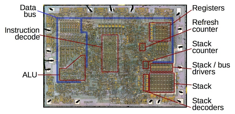
The image below shows the 8008’s tiny silicon die, highly magnified. Around the outside of the die, you can see the 18 wires connecting the die to the chip’s external pins. The 8008’s circuitry is built from about 3500 tiny transistors (yellow) connected by a metal wiring layer (white). This article will focus on the stack circuits on the right side of the chip and how they interact with the data bus (blue).
For the 8008 processor’s birthday, I’m using the date of its first public announcement, an article in Electronics on March 13, 1972 entitled “8-bit parallel processor offered on a single chip.” This article described the 8008 as a complete central processing unit for use in “intelligent terminals” and stated that chips were available at $200 each.1
for more detail: Analyzing the vintage 8008 processor from die photos: its unusual counters
- How many transistors are used in the 8008 processor?
The 8008 circuitry is built from about 3500 tiny transistors. - What makes the 8008 stack implementation unusual compared to modern architectures?
It had an on-chip stack for subroutine calls rather than storing the stack in RAM. - Why did the 8008 use shift-register counters instead of normal binary counters?
The 8008 saved a few gates by using shift-register counters that generated pseudo-random values. - When was the Intel 8008 first publicly announced?
It was first announced on March 13, 1972, in an article in Electronics. - What was the original price of the 8008 chip when it became available?
Chips were initially available at $200 each. - What was the intended use case for the 8008 processor?
It was described as a complete central processing unit for use in intelligent terminals. - How does the article describe the visual appearance of the silicon die?
The die shows 18 wires connecting to external pins with yellow transistors and a white metal wiring layer.