
Summary of 8V97051 Low Power Wideband Fractional RF Synthesizer
This article describes a low-power wideband RF synthesizer design for GSM receiver cards, featuring dual differential/open drain outputs from 34.375MHz to 4400MHz on a 3.3V supply with 1.8V logic compatibility. The system achieves -143dBc/Hz phase noise and includes a mute function via pin or SPI. It integrates an IDT8V97051NLGi PLL/VCO, a temperature-compensated crystal oscillator, various filters, a USB-to-UART/FIFO IC, an I2C-to-SPI bridge IC, and a power supply management section with RC filters.
Parts used in the Low Power Wideband RF Synthesizer:
- IDT8V97051NLGi wideband RF synthesizer/PLL
- Voltage Controlled Oscillator (VCO)
- Temperature compensated crystal oscillator
- Filters (for minimizing undesired noise)
- USB 2.0 high speed to UART/FIFO IC
- I2C-bus to SPI bridge IC
- Power supply management circuitry
- RC filters (on every supply line)
This design features a low power wideband RF synthesizer that is used in GSM receiver cards. It has dual differential and open drain outputs with frequency range of 34.375MHz to 4400MHz(in continuous range). The logic compatibility is 1.8V while the system is running on a single 3.3V supply. It has -143dBc/Hz Phase Noise (PN) performance at 1MHz Offset for every 1.1GHz output. It is also capable of mute function at RF_OUT that is accessible via mute pin or SPI command. It is low power with only 380mW average power consumption while RF_OUTB is not in used.
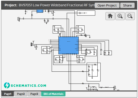
The design is comprised of 3 major parts. The first part consists of IDT8V97051NLGi wideband RF synthesizer/PLL supports the output frequencies with Voltage Controlled Oscillator (VCO). The temperature compensated crystal oscillator close to the RF input helps in the precision of signal while the other parts are filters that are used in various purposes like minimizing undesired noise. The second part consists of the USB 2.0 high speed to UART/FIFO IC that is used for system interface while the I2C-bus to SPI bridge IC controls the sequences, protocol, and timing of the signal. The last part is power supply management of the system in which it is provided with RC filters in every line to ensure minimal noise are included in the supply.
For more detail: 8V97051 Low Power Wideband Fractional RF Synthesizer
-
What is the frequency range of this RF synthesizer?
The device supports a continuous frequency range of 34.375MHz to 4400MHz. -
How much power does the system consume when RF_OUTB is not in use?
The average power consumption is only 380mW when RF_OUTB is not in use. -
Does the design support a mute function at the RF output?
Yes, the mute function at RF_OUT is accessible via a mute pin or an SPI command. -
What voltage levels are used for logic compatibility and system operation?
The logic compatibility is 1.8V while the system runs on a single 3.3V supply. -
How is the precision of the signal ensured in this design?
A temperature compensated crystal oscillator placed close to the RF input helps ensure signal precision. -
Which IC controls the sequences, protocol, and timing of the signal?
An I2C-bus to SPI bridge IC controls the sequences, protocol, and timing of the signal. -
How is noise minimized in the power supply lines?
RC filters are provided on every supply line to ensure minimal noise is included in the supply.