Introduction Especially for switch-mode power supplies (SMPSs), the printed circuit board (PCB) layout is a critical but often under appreciated step in achieving proper performance and reliability. Errors in the PCB layout cause a variety of misbehaviors including poor output voltage regulation, switching jitter, and even device failure. Issues like these should be avoided at all costs, since fixing them usually requires a PCB design modification. However, these pitfalls are easily circumvented if time and thought are spent during the PCB layout process before the first PCBs are ever ordered. This article presents five simple steps to ensure that your next step-down converter’s PCB layout is robust and ready for prototyping. When designing a server, tablet, or electronic point-ofsale machine, a best-practice option with the least risk is to simply copy the PCB layout example found on the evaluation module (EVM) and shown in the datasheet. However, this may not always be possible for various reasons. This article was created for these cases and details a five-step procedure to design a good PCB layout for any TPS62xxx integrated-switch, step-down converter. The internal MOSFETs and integrated loop-compensation circuitry greatly simplify the PCB layout of these devices by reducing the difficulty and time required to do the PCB layout. The versatile TPS62130A is used as the example step-down converter, which can be used in each of the above applications. Figure 1 shows the completed schematic of a typical circuit.
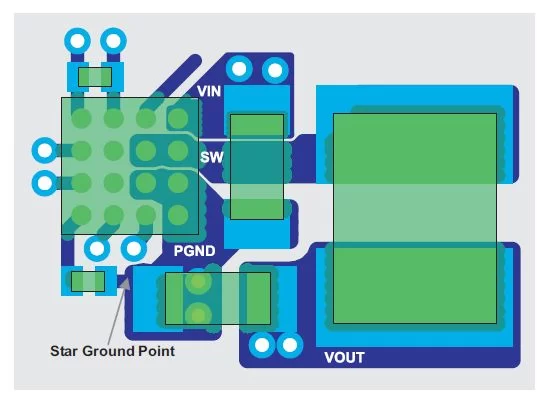
Step #1. Place and route the input capacitor The input capacitor is the single-most important component for reliable operation of any step-down converter. As such, it should be the first component placed in the layout after the IC. Route the capacitor to the IC immediately after it is placed, so that nothing else can be routed in its path. Extra parasitic inductance between the input capacitor’s terminals, both power and ground, and the IC’s PVIN
For more detail: Five steps to a great PCB layout for a step-down converter
About The Author
Ibrar Ayyub
I am an experienced technical writer holding a Master's degree in computer science from BZU Multan, Pakistan University. With a background spanning various industries, particularly in home automation and engineering, I have honed my skills in crafting clear and concise content. Proficient in leveraging infographics and diagrams, I strive to simplify complex concepts for readers. My strength lies in thorough research and presenting information in a structured and logical format.
Follow Us:LinkedinTwitter