
Why op amps are important
Op amps are a key component in analog circuits. An op amp takes two input voltages, subtracts them, multiplies the difference by a huge value (100,000 or more), and outputs the result as a voltage. If you’ve studied analog circuits, op amps will be familiar to you, but otherwise this may seem like a bizarre and pointless device. How often do you need to subtract two voltages? And why amplify by such a huge factor: will a 1 volt input result in lightning shooting from the op amp? The answer is feedback: by using a feedback signal, the output becomes a sensible value and the high amplification makes the circuit performance stable.
Op amps are used as amplifiers, filters, integrators, differentiators, and many other circuits.[2] Op amps are all around you: your computer’s power supply uses op amps for regulation. Your cell phone uses op amps for filtering and amplifying audio signals, camera signals, and the broadcast cell signal.
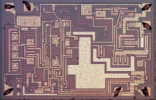
The structure of the integrated circuit
NPN transistors inside the IC
Transistors are the key components in a chip. If you’ve studied electronics, you’ve probably seen a diagram of a NPN transistor like the one below, showing the collector (C), base (B), and emitter (E) of the transistor, The transistor is illustrated as a sandwich of P silicon in between two symmetric layers of N silicon; the N-P-N layers make a NPN transistor. It turns out that transistors on a chip look nothing like this, and the base often isn’t even in the middle!
The photo below shows one of the transistors in the 741 as it appears on the chip. The different brown and purple colors are regions of silicon that has been doped differently, forming N and P regions. The whitish-yellow areas are the metal layer of the chip on top of the silicon – these form the wires connecting to the collector, emitter, and base.
Underneath the photo is a cross-section drawing showing approximately how the transistor is constructed. There’s a lot more than just the N-P-N sandwich you see in books, but if you look carefully at the vertical cross section below the ‘E’, you can find the N-P-N that forms the transistor. The emitter (E) wire is connected to N+ silicon. Below that is a P layer connected to the base contact (B). And below that is a N+ layer connected (indirectly) to the collector (C).[3] The transistor is surrounded by a P+ ring that isolates it from neighboring components.
For more detail: Understanding silicon circuits: inside the ubiquitous 741 op amp
About The Author
Ibrar Ayyub
I am an experienced technical writer holding a Master's degree in computer science from BZU Multan, Pakistan University. With a background spanning various industries, particularly in home automation and engineering, I have honed my skills in crafting clear and concise content. Proficient in leveraging infographics and diagrams, I strive to simplify complex concepts for readers. My strength lies in thorough research and presenting information in a structured and logical format.
Follow Us:LinkedinTwitter