
PORTLAND, Ore. — The world’s most expensive semiconductor fabrication plant–at over $14 billion–was announced at the ground breaking ceremony Thursday (May 7) by Samsung. Located in the Godeok Industrial Complex at Pyeongtaek City Gyeonggi-do Province–called “Samsung Semiconductor Valley”–in South Korea, Samsung will be building 10-nanometer FinFET semiconductors there.
“The new fabrication plant in Pyeongtaek constitutes an important part of our vision to establish a globally balanced semiconductor fabrication network that further solidifies our strong global presence,” Jim Elliott, corporate vice president, Samsung Semiconductor told EE Times. “The plant will play a key role in our future business initiatives, as we continue to invest in areas that contribute much towards our industry leadership.”
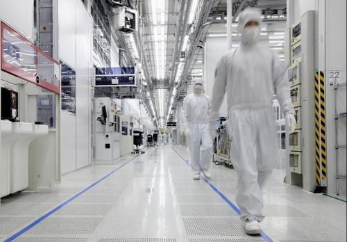 The new plant will be finished in 2017, according to Samsung, and is reported to almost as big–at 31 million square feet plant–as Samsung’s next two biggest fabs put together at Giheung and Hwaseong South Korea. It has been three years since Samsung constructed its last semiconductor fab in Hwaseong. Samsung expects the new plant to have the industry’s largest capacity.
Although Samsung has not yet confirmed what chips will be fabricated there, the new plant is reported to employ about 150,000 people and to produce about $40 billion dollars per year in chip revenue producing DRAMs alone. It is also reported to be targeting the mobile space, server sector and the Internet of Things (IoT)
Samsung reported that its smartphone sales were slumping 20 percent in the fourth quarter of 2014, while its semiconductor sales surged 50 percent. Samsung has since been reported to have surged back in smartphone sales in the first quarter of 2015, however its semiconductor division is still outpacing its smartphones potentially making its investment in a 10 nanometer fab a smart (if expensive) move.
For more detail: Samsung Building World’s Most Expensive Fab for 10-Nanometer FinFETs
About The Author
Ibrar Ayyub
I am an experienced technical writer holding a Master's degree in computer science from BZU Multan, Pakistan University. With a background spanning various industries, particularly in home automation and engineering, I have honed my skills in crafting clear and concise content. Proficient in leveraging infographics and diagrams, I strive to simplify complex concepts for readers. My strength lies in thorough research and presenting information in a structured and logical format.
Follow Us:LinkedinTwitter