
In this instructable I’m going to show you how to make your own PIC18 development board that features both Ethernet and Full Speed USB 2.0 at a low cost.
Features:
The development board is based on a PIC18LF4553 microcontroller. The microcontroller features a Full Speed USB 2.0 (12Mbit/s) interface without the need for any external components. Also, it has 32KB of program memory, 2KB of RAM and it supports an external clock up to 48MHz, which is optional because it also has an 8MHz internal clock.
The ENC28J60 Ethernet controller is used to provide Ethernet connectivity to the microcontroller thought the SPI interface. The ENC28J60 has an integrated MAC and a 10Base-T PHY, 8KB of buffer RAM, supports both Full and Half-Duplex modes and it is fully compatible with 10/100/1000Base-T networks.
The microcontroller is not soldered directly on the PCB but mounted on an IC socket. The advantage of doing this is that when you are done with the development of the code and you want to make a prototype, you can just pop the microcontroller out and make a new PCB with only the components you actually need for your project.
Because the ENC28J60 needs a 3.3V supply to function I decided to power the microcontroller from 3.3V too. That eliminates the need for two different voltage regulators and for logic shifters between the microcontroller and the Ethernet controller. That means reduction of the BOM cost and more space available on the PCB for other components. On the other hand the LF version of a PIC microcontroller can function over an extended VDD range of 2.0V to 5.5V, so if your project needs to run on 5V instead of 3.3V when you move the microcontroller from the development board to a more permanent board you can power it from 5V if you want.
The board can be powered either from the USB port or from an external source from 4.5V up to 12V though the power jack. Keep in mind though that the ENC28J60 can draw up to 180mA so if you try to power the board from a standard 9V battery you may have problems. The selection of the voltage source is done by a jumper.
Step 1: The Parts
To make the development board you will need the following parts:
- 10 x 100nF Ceramic SMD Capacitors (0603 package)
- 2 x 10uF Tantalum SMD Capacitors (3528 package)
- 4 x 22pF Ceramic SMD Capacitors (0805 package)
- 1 x PIC18LF4553 or PIC18LF4550 (PDIP package) – I recommend using a PIC18LF4553 because it has a 12 bit ADC (which is basically the only difference between the two). The PIC18LF445x microcontrollers are also compatible with the board but they have 24KB of program memory instead of 32KB.
- 1 x 40 pin PDIP IC Socket
- 1 x ENC28J60 (SPDIP package)
- 1 x MagJack RJ45 Connector – The particular I used is this, but you can use any MagJack compatible connector as long as it has the same footprint. I also found an alternative on eBay which is called HR911105A but I never tried it.
- 1 x DC Barrel Jack 5.5mm (Through hole)
- 1 x USB Mini-B SMD Connector
- 1 x 25MHz XTAL SMD (HC49/UP package)
- 1 x 8MHz XTAL SMD (HC49/UP package) – I used an 8MHz XTAL but any XTAL up to 48MHz will work.
- 2 x 10K SMD Resistors (0805 package)
- 8 x 100Ω SMD Resistors (0805 package) – 1% tolerance if possible.
- 1 x 1.5K SMD Resistor (0805 package)
- 1 x 2.2K SMD Resistor (0805 package) – 1% tolerance if possible.
- 1 x 120Ω SMD Resistor (0805 package) – 1% tolerance if possible.
- 2 x 470Ω SMD Resistors (0805 package)
- 1 x Momentary SMD Switch – The particular I used is this, but you can use any momentary switch you want with the same footprint.
- 1 x Ferrite Bead rated for at least 80mA (Through hole) – If you can’t find one you can make one yourself using a small toroid ferrite core and a little solid core wire (like I did). Five to six turns is all you need.
- 1 x LD1117V33 SMD Voltage Regulator, also known as LD33 (SOT223 package)
- 1 x 2.54mm (100mil) 40-pin Male Pin Header (Through hole) – You will need to cut it to smaller pieces.
- 1 x 2.54mm (100mil) 4×2-pin Male Pin Header (Through hole)
- 1 x 2.54mm (100mil) 40-pin Female Pin Header (Through hole) – You will need to cut it to smaller pieces.
- Solid core wire to use it for the jumpers on the PCB – To fit the holes on the PCB the copper inside the wire needs to be around 0.65mm (22 AWG). A slight thicker solid core wire should also work.
- 1 x 80x62mm PCB – Photoresist or bare copper depending on the etching method you are going to use.
- 1 x 2.54mm (100mil) jumper – The same like the ones that are used on computer motherboards.
Optional Parts:
- 4 x Female to Female Brass Standoff Spacers
- 4 x Screws for the Spacers
The BOM cost will be around 13€ to 15€ ($14.8 to $17) depending from where you’ll buy the parts. Most of the parts can be found easily on eBay.
Step 2: Making the PCB
The next step is to make the PCB. Because this is not a tutorial about PCB etching I’m not going to get into details about the process, but instead I’m going to give you some guidelines specific to this project.
[ Credits to Chris Meletis for the PCB layout ]
Etching the PCB:
Before you choose the etching method you want to follow keep in mind that some traces have a clearance of 0.3mm (12mil) so if you try use the toner transfer method you might experience some issues. I don’t say it’s not possible but it will definitely be more difficult than the photoresist method to get a good result. Personally, I used the photoresist method and the result was great on the first try. I only had a minor issue with one of the traces, but that was caused by a clearance error on the layout not by the etching process itself. Now the layout has been corrected so you won’t have any issues.
If you choose the photoresist method, about the exposure make sure to use only one high resolution transparency otherwise you might fail to expose correctly the traces that have very small clearance and/or the thermal pads. I had great success using a good inkjet printer and high resolution inkjet transparencies. The transparencies were a little expensive but worth every cent.
About the development of the PCB, the trick to know when you are done is to wait for the thermal pads to show up. When you are able to see the thermal pads then you know that the board is ready for etching.
Drilling the Holes:
After you etch the PCB you will have to drill the holes for the through hole components. Most of the holes need either a 0.8mm or a 1mm drill bit. The holes for the ICs and the ferrite bead are 0.8mm. The holes for the pin headers and the jumper wires are 1mm. The MagJack connector has 2 holes that are 1.6mm for the shield ground and 2 for the plastics that are 3.2mm, the rest are 1mm. The barrel jack needs 3 holes with a diameter of 3.2mm. The Mini-B USB connector needs two 0.9mm holes, that don’t have to go all the way though the PCB but only half way. If you don’t have a 0.9mm drill bit then an 1mm bit will work fine. Finally, the board also has 4 mounting holes 3.2mm each on the edges that is up to you if you want to drill them.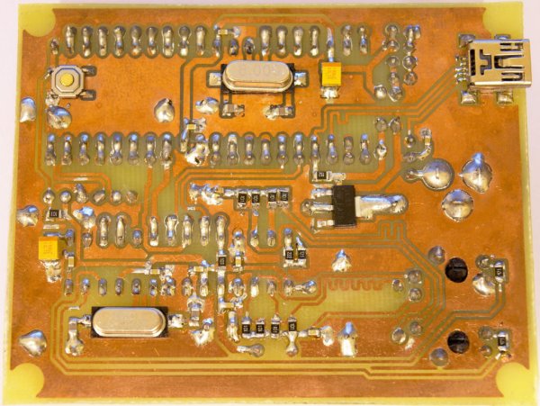
Step 3: Soldering the Components
After drilling the holes it’s time for the fun part, to solder the components on the PCB. Most of the components are SMD so you gonna need a little bit of flux to assist you and of course a pair of tweezers. Start by soldering all the 100nF capacitors first since they are the smallest of all the components. After the 0603 capacitors, go for all the 0805 components and after that for the two 3528 tantalum capacitors. Finally, solder the crystals, the USB port and the momentary switch and you are done with the SMD components.
When you are finished soldering the SMD components it’s time for the through hole. Note that all the through hole components are mirrored on the PCB layout so they need to be soldered on the non copper side of the PCB. Also, note that there are two jumpers under the microcontroller. You will need to solder them first before you solder the IC socket.
Before soldering the MagJack connector you will have first to cut the pins 4, 5 and 6 because since they are not used they were omitted on the board layout in favor of some extra space for the traces.
Furthermore, because the ENC28J60 unlike the microcontroller needs to dissipate a fair amount of heat, it needs to be soldered directly on the PCB without a socket. That way the copper of the ground plane will act as a heat sink and will dissipate an amount of heat. Another reason you want to solder the ENC28J60 directly on the PCB is to minimize the parasitic capacitance and inductance which can introduce noise.
Finally, on the trace that is connected with the top pad of the voltage regulator make sure to add a fair amount of solder. This is going to help a lot with the heat dissipation of the regulator.
When you are done with the soldering don’t forget to clean the PCB from the flux residue. If you use rosin flux then isopropyl alcohol is all you need.
The last thing you need to do after soldering is to put the jumper on the pin header that selects the voltage source.
For more detail: PIC18 Development Board with Ethernet and USB
About The Author
Ibrar Ayyub
I am an experienced technical writer holding a Master's degree in computer science from BZU Multan, Pakistan University. With a background spanning various industries, particularly in home automation and engineering, I have honed my skills in crafting clear and concise content. Proficient in leveraging infographics and diagrams, I strive to simplify complex concepts for readers. My strength lies in thorough research and presenting information in a structured and logical format.
Follow Us:LinkedinTwitter