
We have been wanting to design and build an open-design, relatively inexpensive but fully functioned charge regulator for solar PV, wind, pedal and small hydro systems for a while now.
The majority of off-grid renewable energy systems are based upon lead acid batteries. Lead-acid batteries need to be protected from over-charging by the renewable energy source and over-discharging from the loads. This can be one with a series regulator (in the case of solar PV) or a shunt regulator (for PV, hydro and wind). Please check the web or my electrical design guide in the information section for more details.

This post is a collection of a design ideas and background to the subject. I’ll be updating this as I go along – I’d really like to know your thoughts and ideas.
Design specifications:
- Battery bank nominal voltage: 12 – 24 DC, up to 48V would be good.
- Actual voltage range: 10-32V DC, or up to 65V DC for 48V system.
- Current range: 0 – 20A DC
- Required options (must have):
- Battery voltage indication,
- Adjustable set-points (different types of batteries)
- Reverse polarity protection
- Over current protection
- Useful options (nice to have):
- Could be either series or shunt regulator,
- Low Voltage Disconnect,
- Voltage display,
- Current display,
- On-board data storage,
- Maximum power point tracking,
- Over voltage protection
Available designs
The initial starting point for all projects nowadays is to do a trawl of the web. Here is a brief list of the projects I found. I am mainly interested in open-source projects, but the ideas and costs of others is also useful.
- Commercial manufactured units
Typical prices are in the range of £10 (eBay cheapest) to £200. Basic designs do not have a low voltage disconnect, nor V or I monitoring.
This looks like a really interesting project, with plans to build an open source maximum power point tracking charge controller for solar PV (and wind) systems.
12V and 24V versions. Cost is $14.50 + P&P, from USA. Based upon the ZM33064 voltage controlled switch, with a IRFZ44N mosfet to control the dump load. Hysteresis is controlled with a resistor value. No dump load is included (it must have this to function).
This is a PIC microcontroller based PWM solar charge regulator. UK designed and made. £17.99. Simple in-line series regulator for PV up to 100Wp, 12 or 24V. One LED to display function. Information about the design of the device is on the website, but I could not find the full design details.
(Edit 15/11/12: The circuit schematics have been made available: http://www.256.co.uk/?p=917)
A number of electronic circuits with a couple of solar regulator circuits (one and two). Relatively simple circuits. Full circuit diagrams.
Another reltively simple design (from an edition of ETI (Electronics Today International). Uses a 555 timer. For a 5W solar panel.
A simple PWM series regulator from an article in Elektor Electronic magazine, March 2000. This is for 12V panels up to 53Wp. I have made a number of these and they work well. They do not give enough information about the battery voltage.
Only for very small solar panels.
A load of solar circuits, mainly relating to solar tracking.
Based upon the LM2575T-ADJ switching regulator. Design is only OK for up to 1A, but is a switching regulator so should have very good efficiency.
- Arduino-based solar charge regulators
timnolan – a hill-climbing maximum power point tracking solar PV regulator.
This uses realys to control the dump load and the supply.
Uses a realy to control a dump load
Initial design
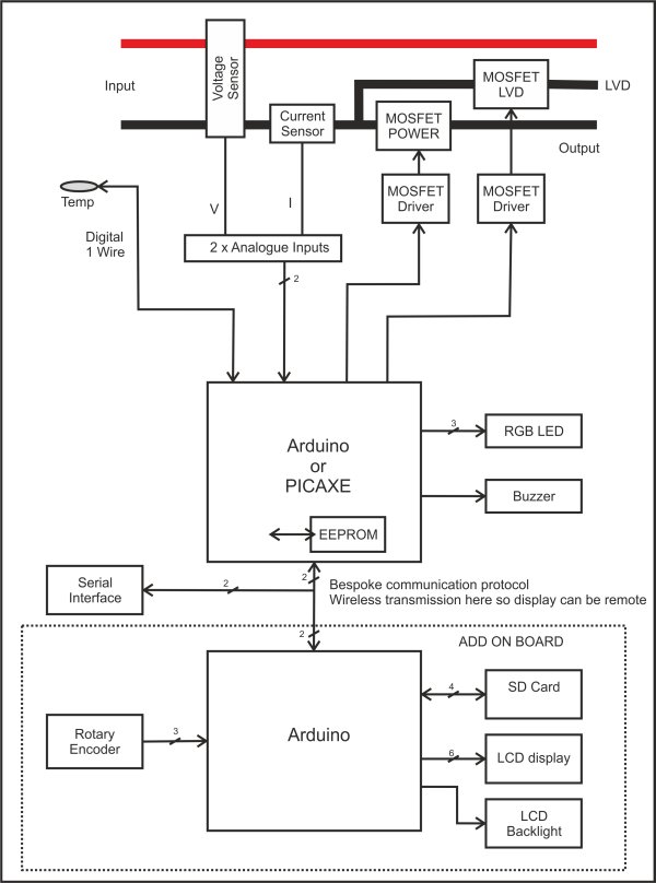
There are five main parts to the system:
- Voltage monitoring – monitors the voltage
- Microcontoller – the ‘brains’ of the device. This will make decisions based upon the voltage monitoring to control the power stage.
- Power stage – this will control the power from the solar panel, by either series or shunt regulation.
- Display – LEDs will show the system status. This could also be an LCD display.
- Power supply – to convert the incomming voltage to the circuit voltage (5V). Must be efficient.
- Current monitoring – for information and user interface (added 27/6/12)
An overview of the system is here (27/6/12):
This has been updated from the original idea to make it more versatile and to include either PICAXE or Arduino microcontroller systems. The plan is to have a basic board with the power supply, power electronic components, voltage and current monitoring which would work as a stand alone unit.
A display and data aquisition board can then be easily slotted in to expand the system, if required, but would not be required for basic operation. This will include another microporcessor, most probably based upon the Arduino, which will control an LCD display and SD card data storage.
This adds current monitoring to the list of things to investigate.
Update 11/12/12: High-side MOSFET switching will be used on the input. This will allow a common negative connection which will be easier to implement and is more standard.
Voltage monitoring
This is done through a simple voltage divider circuit. Zener diodes ensure that the inputs to the microcontroller are protected.
The input voltage is read via a potential divider. Initially the maximum voltage will be 32V dc (this is for a fully charged 24V system). The maximum input to the PICAXE is 5V, so we need to convert 32V to 5V, at a very low current. Check here for the theory. If we use 10kΩ as the lower resistor (R1), then R2 is 54kΩ. The standard resistor value near to 54k is 56k Ω, so lets use that value. Total resistance is 66kΩ, so at 32V the current is 0.5mA, consuming 0.0165W (16.5mW). We could change this to 100kΩ and 560kΩ for even lower power consumption.
Here is a schematic diagram, but with a 680k resistor, rather than a 560k:
We need to think about the resolution of this. The PICAXE only has an 8-bit ADC, hence the 5V input is converted into 28 levels (256 levels). Each inout level is equivalent to 5/256 = 0.01953V (19.5mV). This goes through th potential divider to give the voltage level steps of 0.01953 x ((56+10)/10) = 0.128V (128mV). This is OK but not great. The PICAXE can also do 10 bit resolution using the command adcread10. This requires 2 bytes to hold the information (210 levels = 1024 levels). I will use this command in the code.
A 5V1 zener diode protect the input to the PICAXE from any spikes or over voltage. A 0.1uF/100nF capacitor smooths the signal to stop any fast variation.
EDIT 16/8/13
Please see my voltage monitoring and accurate voltage monitoring posts.
Current Monitoring
While not strictly necessary for regulation (most charge controllers just use voltage regulation), measuring current is a very useful system parameter and allows lots more decisions to be made and scope for expansion. It is also a very useful parameter to know what is going on within the system and allows us to display the input power from the multiplication of voltage and current.
I have posted some work on current monitoring here. I will narrow down th choices based upon accuracy, cost and component availability and place the final design here.
Here is an application note from Maxim on high-side current monitoring.
Microcontroller
This design will be micro-controller based. this means that people can load their own code onto the system, in case they would like to change any of the functions. I have been using a number of microcontrollers including PICs, ATMEL, Arduino boards and PICAXE chips. I wanted to make the design suitable for a wide range of people and not limit the design to any one particular microconroller or system. For this reason I have now decideed to make the system compatible with the PICAXE and the Arduino which means it will also be compatible with PIC microcontrollers and Atmel microcontrollers.
PICAXE
I have been impressed with the PICAXE as an inexpensive, but very easy to use and program. The programming environment is free and the programming cable is very cheap (I made my own using parts from my junk box). The only issue is that the bootloader is not open-source. The cost of a PICAXE is low and very close to the part cost of the actual PIC.
The PICAXE system is not open source, though.
I am basing this deign on the PICAXE 14M02. This component has 12 input/output pins, of which 7 can be analogue channels. This component can also support parallel tasks, 6 PWM outputs and touch sensors.
The various I/O require are:
- Voltage – INPUT – ADC
- Current – INPUT – ADC (future use)
- LED Red – OUTPUT – PWM
- LED Blue – OUTPUT – PWM
- LED Green – OUTPUT – PWM
- Power stage – OUTPUT – PWM
- LVD stage – OUTPUT – PWM (future use)
- Serial IN – INPUT
- Serial OUT – OUTPUT
- SD card storage – 3 lines required. Use SPI? (future use)
- SD card storage – 3 lines required. Use SPI? (future use)
- SD card storage – 3 lines required. Use SPI? (future use)
And that is the full quota of I/O pins on the PICAXE 14M2. This component could be changed for another part as the project moves along – but its better to get something going and working.
ARDUINO
Update 27/6/12: As can be seen from the new overview at the start of this article I have decided to make the design both PICAXE and Arduino compatible.
The Arduino is a ubiquitous microcontroller system based upon the Atmel ATmega 328 microcontroller. It has an amazing amount of code examples and a huge user base. It is all totally free and open source. Check out the huge array of Arduino projects out there for more information. At the beginning of this project I did think that it was over-specified for this project but as I have moved further then I have been basing more and more of my work on the Arduino and feel that it is suitable for this project.
The Arduino is basically a boot loader and programming environment for the Atmel ATmega328 microcontroller.
Power stage
A 20A or higher MOSFET will be used to control the output power stage. This must have the correct driving circuitry (enough current reserves to switch on and off fully). This will be pulse width modulated to control the power from the PV module.
Initially I chose to use low side MOSFET driver circuits. The main problem with this is that the ground of the solar PV panel and the battery cannot be directly connected. This could be an issue in some situations. Hence I plan on using high side MOSFET driver. The low side FET driving has been left for information and it will also be used for the low voltage disconnect.
LOW SIDE FET DRIVING
For the prototype I am using a logic level driven MOSFET (type IRL520N), but this is only a 10A rated device. The series resistor helps ensure that there is less of a switch ON spike. The gate-to-ground resistor ensures the MOSFET switches fully OFF. The diode (this should be a high speed diode NOT the 1N4001 shown here (see below)) allows any current to flow away when the FET is switched OFF, otherwise there would be a spike on switch OFF.
This works OK but when viewed on an oscilloscope there were very high voltage spikes when the FET was switched ON. This is unusual and must be caused by a change in current and it not having anywhere to go. The voltage spike is in the region of 60V for a 12V system, so pretty high. Ideas on why this is happening are:
- Its a measurement error
- The diode is not fast enough
- The load has a very large inductance (though this should not matter with the diode)
12/1/12 Update: There was a high voltage spike during the MOSFET switch OFF. This is seen when the current in the load has nowhere to go. I mis-read this by connecting up the ‘scope incorrectly and I thought it was a spike at switch ON, which would be very unusual.
The reason for the OFF voltage spike was the fact I was using a ‘regular’ low frequency (50Hz) rectifier diode (1N4001), rather than a high speed diode (type 1N4937). When replaced with a high speed diode everything looked a lot better with virtually no spike seen.
MOSFET CHOICE
There are loads of MOSFETs to choose from. In this application we have set the prarmeters that it must be N-channel, able to cope with 20A continuous drain current and have a relatively low ON resistance (hence low power loss). The initial design used a 10A logic level MOSFET. This was running too hot when using a 12A load, as you would expect. So I had a look for suitable replacements:
- STP24NF10 – not yet tested in this design
- PHP50N06 – 52A, 0.028Ω, TO220 package, not availble RS/Farnell, not yet tested
- 75337P – 75A, 0.014Ω, TO220 package, not available RS/Farnell, not yet tested
- HUF75339P3 – 75A, 0.012Ω, TO220, Farnell cost = £0.81, not yet tested in this design
- IRLI3705N – 52A, 0.01Ω, TO220, RS cost = £1.47
Changing MOSFETs fom the logic level 10A one to a ‘normal’ requires a bit more than just replacing the component in the circuit. We are trying to interface a 0-5V digital signal to the MOSFET so it can switch up to 20A. MOSFETs are voltage-controlled current sources, which means they switch on when a voltage is applied, but that is a bit of a generalisation. Within the MOSFET there is a parasitic capacitance, which means we do need to supply and remove current to the gate to switch the device on and off. Also we need to supply enough voltage to fully switch ON the MOSFET (as we are using it as a switch). If we only apply 5V then we may not switch the device fully ON – we should really apply a higher voltage (typically to fully switch ON a power FET we need to have the gate voltage at least 10V higher than the source voltage (Vgs)). Also we need to supply some current. The microcontroller can probably do this but switching at high speed might mean the microcontroller cannot supply enough current for correct switching. To do this we need to three choices – we can use a logic level FET, we can use a FET driver or we can build our own driver from an additional transistor. The first option adds some cost, but might be a good option in the future. The second option adds an additional part which is typically non-standard. The second option is how I will move forwards with this prototype, as it is the fastest option to get working.
When tested the microcontroller output pin was connected directly to the MOSFET gate pin. This switched the FET fully on and off when there was no load.
For more detail: OPEN-DESIGN CHARGE REGULATOR PROJECT
About The Author
Ibrar Ayyub
I am an experienced technical writer holding a Master's degree in computer science from BZU Multan, Pakistan University. With a background spanning various industries, particularly in home automation and engineering, I have honed my skills in crafting clear and concise content. Proficient in leveraging infographics and diagrams, I strive to simplify complex concepts for readers. My strength lies in thorough research and presenting information in a structured and logical format.
Follow Us:LinkedinTwitter