
PORTLAND, Ore. — Every semiconductor research organization in the world is trying to fabricate single monolayers of graphene and pattern them in such a way as to make superior circuitry to silicon. Now, however, some of the IBM researchers who have been growing monolayers of graphene have found another advantageous use for them- — one that greatly lowers the cost of fabricating blue light emitting diodes (LEDs) from gallium nitride (GaN).
“We grew a single-crystalline gallium nitride [GaN] film on wafer-scale graphene formed on a silicon carbide (SiC) wafer,” the self-described “Master Inventor” and Research Staff Member at IBM’s T.J. Watson Research Center (Yorktown Heights, New York), Jeehwan Kim, told EE Times.
“An entire GaN film was then transferred to a silicon [Si] substrate and the graphene which remained on the SiC wafer was reused multiple times to grow and transfer multiple GaN films. In principle, this method can be much more cost-effective compared to conventional methods where an expensive SiC wafer or sapphire wafer is used only one time to grow GaN films without reusability. Also we found that the film quality is higher on graphene than other substrates (less defect density) Therefore, our technique offers extreme cost-efficiency and better overlaying film quality.”
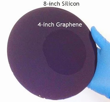
It has been extremely challenging to grow graphene monolayer films on a wafer scale, but boiling off the silicon from a silicon carbide wafer has been found to be one of the most reliable methods. For fabricating circuitry using graphene as the semiconductor many different methods have been tried in the past, most only partially successful. In fact, Kim has also demonstrated that graphene films obtained by boiling off the Si from SiC wafers can be reliably transferred to silicon substrates (see illustration) as well as demonstrated that their quality was higher than trying to grow graphene in-place on the wafer where it will be used.
For more detail: IBM Grows Wafer Scale Graphene
About The Author
Ibrar Ayyub
I am an experienced technical writer holding a Master's degree in computer science from BZU Multan, Pakistan University. With a background spanning various industries, particularly in home automation and engineering, I have honed my skills in crafting clear and concise content. Proficient in leveraging infographics and diagrams, I strive to simplify complex concepts for readers. My strength lies in thorough research and presenting information in a structured and logical format.
Follow Us:LinkedinTwitter