A microcontroller, a digital device, can read, execute and transmit only digital signals. On the contrary, the outputs of the most of the transducers are analog in nature. Thus it is hard to interface these transducers directly with controllers. Analog-to-digital convertor (ADC) ICs are one way to make the analog input compatible with the microcontroller.
Using an external ADC adds complexity to the circuit. To avoid this complexity, PIC Microcontrollers have in-built ADC module which reduces the cost and connections of the circuit. This article explains the in-built ADC of PIC18F4550 controller.
As mentioned in the summary, a PIC microcontroller has inbuilt ADC for A/D conversion. The ADC module of PIC18F4550 controller has following specifications:
|
Bit 7
|
Bit 6
|
Bit 5
|
Bit 4
|
Bit 3
|
Bit 2
|
Bit 1
|
Bit 0
|
|
—
|
—
|
CHS3
|
CHS2
|
CHS1
|
CHS0
|
GO/DONE
|
ADON
|
|
CHS3:CHS0
|
Analog Channel
|
Pin
|
|
0000
|
Channel 0
|
RA0/AN0
|
|
0001
|
Channel 1
|
RA1/AN1
|
|
0010
|
Channel 2
|
RA2/AN2
|
|
0011
|
Channel 3
|
RA3/AN3
|
|
0100
|
Channel 4
|
RA5/AN4
|
|
0101
|
Channel 5
|
RE0/AN5
|
|
0110
|
Channel 6
|
RE1/AN6
|
|
0111
|
Channel 7
|
RE2/AN7
|
|
1000
|
Channel 8
|
RB2/AN8
|
|
1001
|
Channel 9
|
RB3/AN9
|
|
1010
|
Channel 10
|
RB1/AN10
|
|
1011
|
Channel 11
|
RB4/AN11
|
|
1100
|
Channel 12
|
RB0/AN12
|
|
Bit 7
|
Bit 6
|
Bit 5
|
Bit 4
|
Bit 3
|
Bit 2
|
Bit 1
|
Bit 0
|
|
—
|
—
|
VCFG1
|
VCFG0
|
PCFG3
|
PCFG2
|
PCFG1
|
PCFG0
|
|
PCFG3:
PCFG0
|
AN12
|
AN11
|
AN10
|
AN9
|
AN8
|
AN7
|
AN6
|
AN5
|
AN4
|
AN3
|
AN2
|
AN1
|
AN0
|
|
0000
|
A
|
A
|
A
|
A
|
A
|
A
|
A
|
A
|
A
|
A
|
A
|
A
|
A
|
|
0001
|
A
|
A
|
A
|
A
|
A
|
A
|
A
|
A
|
A
|
A
|
A
|
A
|
A
|
|
0010
|
A
|
A
|
A
|
A
|
A
|
A
|
A
|
A
|
A
|
A
|
A
|
A
|
A
|
|
0011
|
D
|
A
|
A
|
A
|
A
|
A
|
A
|
A
|
A
|
A
|
A
|
A
|
A
|
|
0100
|
D
|
D
|
A
|
A
|
A
|
A
|
A
|
A
|
A
|
A
|
A
|
A
|
A
|
|
0101
|
D
|
D
|
D
|
A
|
A
|
A
|
A
|
A
|
A
|
A
|
A
|
A
|
A
|
|
0110
|
D
|
D
|
D
|
D
|
A
|
A
|
A
|
A
|
A
|
A
|
A
|
A
|
A
|
|
0111
|
D
|
D
|
D
|
D
|
D
|
A
|
A
|
A
|
A
|
A
|
A
|
A
|
A
|
|
1000
|
D
|
D
|
D
|
D
|
D
|
D
|
A
|
A
|
A
|
A
|
A
|
A
|
A
|
|
1001
|
D
|
D
|
D
|
D
|
D
|
D
|
D
|
A
|
A
|
A
|
A
|
A
|
A
|
|
1010
|
D
|
D
|
D
|
D
|
D
|
D
|
D
|
D
|
A
|
A
|
A
|
A
|
A
|
|
1011
|
D
|
D
|
D
|
D
|
D
|
D
|
D
|
D
|
D
|
A
|
A
|
A
|
A
|
|
1100
|
D
|
D
|
D
|
D
|
D
|
D
|
D
|
D
|
D
|
D
|
A
|
A
|
A
|
|
1101
|
D
|
D
|
D
|
D
|
D
|
D
|
D
|
D
|
D
|
D
|
D
|
A
|
A
|
|
1110
|
D
|
D
|
D
|
D
|
D
|
D
|
D
|
D
|
D
|
D
|
D
|
D
|
A
|
|
1111
|
D
|
D
|
D
|
D
|
D
|
D
|
D
|
D
|
D
|
D
|
D
|
D
|
D
|
|
Bit
|
= 1
|
= 0
|
|
VCGF0
|
Vref+ (RA3)
|
Vcc
|
|
VCGF1
|
Vref- (RA2)
|
Vss (GND)
|
|
Bit 7
|
Bit 6
|
Bit 5
|
Bit 4
|
Bit 3
|
Bit 2
|
Bit 1
|
Bit 0
|
|
ADFM
|
—
|
ACQT2
|
ACQT1
|
ACQT0
|
ADCS2
|
ADCS1
|
ADCS0
|
|
ADCS2:ADCS0
|
Clock Option
|
|
000
|
FRC (clock derived from A/D RC oscillator)
|
|
001
|
FOSC/64
|
|
010
|
FOSC/16
|
|
011
|
FOSC/4
|
|
100
|
FRC (clock derived from A/D RC oscillator)
|
|
101
|
FOSC/32
|
|
110
|
FOSC/8
|
|
111
|
FOSC/2
|

Project Source Code
###
// Program to depict working with inbuilt ADC of PIC18F4550 Microcontroller
// This code uses Channel0 (zero) of PIC’s ADC Module
// Configuration bits
/* _CPUDIV_OSC1_PLL2_1L, // Divide clock by 2
_FOSC_HS_1H, // Select High Speed (HS) oscillator
_WDT_OFF_2H, // Watchdog Timer off
MCLRE_ON_3H // Master Clear on
*/
#define rs LATA.F0
#define rw LATA.F1
#define en LATA.F2
#define lcdport LATB
void lcd_ini();
void lcdcmd(unsigned char);
void lcddata(unsigned char);
void adc_con(unsigned int);
void adc_init();
unsigned char data[20]=”ADC OUTPUT=”;
unsigned int digital_out[10],avg_output=0,temp;
unsigned int i=0;
void main()
{
TRISA=0x01; // Configure RA0 as input pin
LATA=0;
TRISB=0; // Configure Port B as output port
LATB=0;
TRISD=0;
LATD=0;
lcd_ini(); // LCD initialization
while(data[i]!=”)
{
lcddata(data[i]); // Call lcddata function to send character one by from ‘data’ array
i++;
}
adc_init(); //ADC Initialization
while(1)
{
temp=0;
for(i=0;i<10;i++)
{
ADCON0|=(1<<GO); // Start A/D conversion
while(!(ADCON0 & (1<<GO))); // Wait until conversion gets over
digital_out[i]=((ADRESL)|(ADRESH<<8)); // Store 10-bit output into a 16-bit variable
Delay_ms(20);
temp=temp+digital_out[i];
}
avg_output=temp/10; // Take average of ten digital values for stablity
adc_con(avg_output); // Function to convert the decimal vaule to its corresponding ASCII
}
}
void adc_init()
{
ADCON1=0x0E; // Make RA0/AN0 pin as analog pin (Other pins remain to be digital I/O)
ADCON0=0x00; // Select Channel0 & ADC off
ADCON2=0x8A; // Left justified, 2TAD acquiciation time, Fosc/32 clock option
ADCON0.ADON=1; // Enable ADC
}
void lcd_ini()
{
lcdcmd(0x38); // Configure the LCD in 8-bit mode, 2 line and 5×7 font
lcdcmd(0x0C); // Display On and Cursor Off
lcdcmd(0x01); // Clear display screen
lcdcmd(0x06); // Increment cursor
lcdcmd(0x80); // Set cursor position to 1st line, 1st column
}
void adc_con(unsigned int adc_out)
{
unsigned int adc_out1;
int i=0;
char position=0xC3;
for(i=0;i<=3;i++)
{
adc_out1=adc_out%10; // To exract the unit position digit
adc_out=adc_out/10;
lcdcmd(position);
lcddata(48+adc_out1); // Convert into its corresponding ASCII
position–;
}
}
void lcdcmd(unsigned char cmdout)
{
lcdport=cmdout; //Send command to lcdport=PORTB
rs=0;
rw=0;
en=1;
Delay_ms(10);
en=0;
}
void lcddata(unsigned char dataout)
{
lcdport=dataout; //Send data to lcdport=PORTB
rs=1;
rw=0;
en=1;
Delay_ms(10);
en=0;
}
###
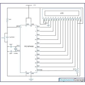
Circuit Diagrams
Project Components
Project Video
Source: How to work with inbuilt ADC Module of PIC Microcontroller (PIC18F4550)
About The Author
Muhammad Bilal
I am a highly skilled and motivated individual with a Master's degree in Computer Science. I have extensive experience in technical writing and a deep understanding of SEO practices.