If you’ve played around with electronic circuits, you probably know[1] the 555 timer integrated circuit, said to be the world’s best-selling integrated circuit with billions sold. Designed by analog IC wizard Hans Camenzind[2] in 1970, the 555 has been called one of the greatest chips of all time with whole books devoted to 555 timer circuits.
Given the popularity of the 555 timer, I thought it would be interesting to find out what’s inside the 555 timer and how it works. While the 555 timer is usually sold as a black plastic IC, it is also available in a metal can, which can be cut open with a hacksaw[3] revealing the tiny die inside.
A brief explanation of the 555 timer
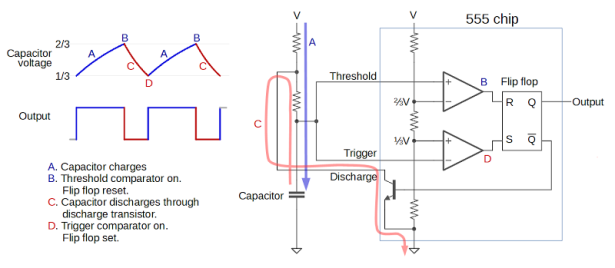
The 555 timer has hundreds of applications, operating as anything from a timer or latch to a voltage-controlled oscillator or modulator. The diagram below illustrates how the 555 timer operates as a simple oscillator. Inside the 555 chip, three resistors form a divider generating references voltages of 1/3 and 2/3 of the supply voltage. The external capacitor will charge and discharge between these limits, producing an oscillation. In more detail, the capacitor will slowly charge (A) through the external resistors until its voltage hits the 2/3 reference. At that point (B), the upper (threshold) comparator switches the flip flop off and the output off. This turns on the discharge transistor, slowly discharging the capacitor (C). When the voltage on the capacitor hits the 1/3 reference (D), the lower (trigger) comparator turns on, setting the flip flop and the output, and the cycle repeats. The values of the resistors and capacitor control the timing, from microseconds to hours.[4]
To summarize, the key components of the 555 timer are the comparators to detect the upper and lower voltage limits, the three-resistor divider to set these limits, and the flip flop to keep track of whether the circuit is charging or discharging. The 555 timer has two other pins (reset and control voltage) that I haven’t covered above; they can be used for more complex circuits.
The structure of the integrated circuit
The photo below shows the silicon die of the 555 through a microscope. On top of the silicon, a thin layer of metal connects different parts of the chip. This metal is clearly visible in the photo as yellowish-white traces and regions. Under the metal, a thin, glassy silicon dioxide layer provides insulation between the metal and the silicon, except where contact holes in the silicon dioxide allow the metal to connect to the silicon. At the edge of the chip, thin wires connect the metal pads to the chip’s external pins.
The different types of silicon on the chip are harder to see. Regions of the chip are treated (doped) with impurities to change the electrical properties of the silicon. N-type silicon has an excess of electrons (negative), while P-type silicon lacks electrons (positive). In the photo, these regions show up as a slightly different color surrounded by a thin black border. These regions are the building blocks of the chip, forming transistors and resistors.
NPN transistors inside the IC
Transistors are the key components in a chip. The 555 timer uses NPN and PNP bipolar transistors. If you’ve studied electronics, you’ve probably seen a diagram of an NPN transistor like the one below, showing the collector (C), base (B), and emitter (E) of the transistor, The transistor is illustrated as a sandwich of P silicon in between two symmetric layers of N silicon; the N-P-N layers make an NPN transistor. It turns out that transistors on a chip look nothing like this, and the base often isn’t even in the middle!
For more detail: 555 timer teardown: inside the world’s most popular IC


